Organic electroluminescence display

a technology of electroluminescence display and organic material, applied in the direction of instruments, static indicating devices, etc., can solve the problems of inability to perform appropriate feedback to image data, meaningless feedback, etc., and achieve the effect of eliminating line memory

Inactive Publication Date: 2008-09-11
JAPAN DISPLAY INC
View PDF22 Cites 71 Cited by
  • Summary
  • Abstract
  • Description
  • Claims
  • Application Information

AI Technical Summary

Benefits of technology

[0012]It is an object of the present invention to eliminate the influence of the temperature difference between the points inside and outside the display area resulting from the comparison between OLED devices of adjacent pixels in the display area with respect to the deterioration of the OLED device over time rather than the comparison with the OLED device of the reference pixel outside the display area.
[0029]In the aspect of the present invention, at each detection of the property of the OLED device of the specific pixel, the determination is made with respect to the abnormality of the pixel as well as performing the burn-in detection. This makes it possible to eliminate the line memory.

Problems solved by technology

However, the aforementioned documents disclose no basis, based on which the OLED device property change is measured.
This may fail to display the correct image, thus making the feedback meaningless.
The reference pixel may change over time, and in such a case, the basis may be changed, thus failing to perform the appropriate feedback.
The appropriate feedback to the image data cannot be performed unless the difference is appropriately corrected.

Method used


Image

  • Organic electroluminescence display
  • Organic electroluminescence display
  • Organic electroluminescence display

Examples


first embodiment

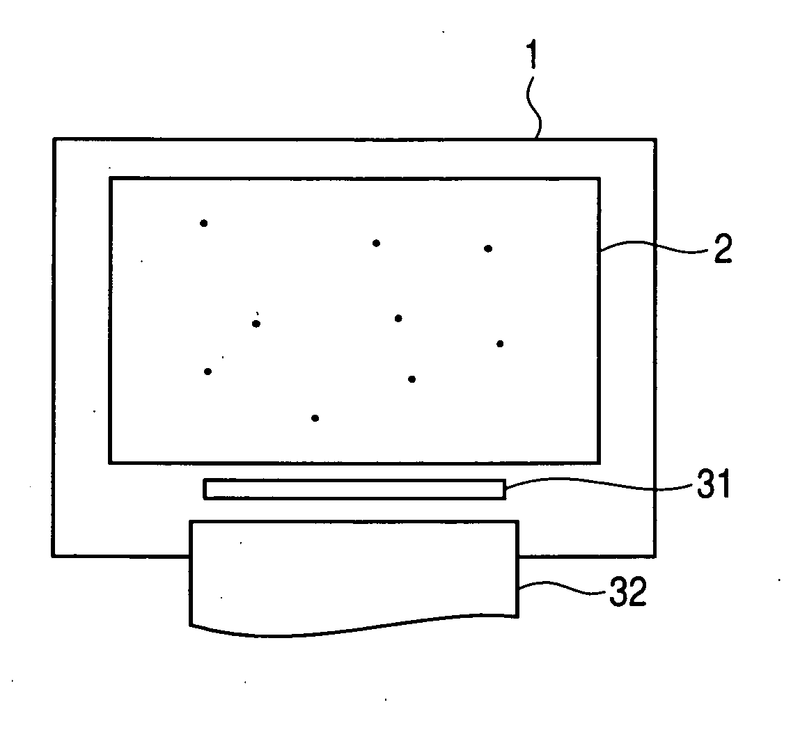
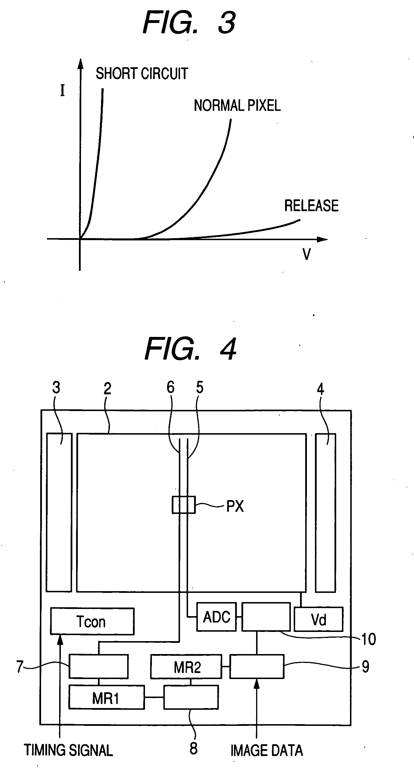
[0049]FIG. 1 shows an example of an organic electroluminescence display unit according to the present invention. Referring to FIG. 1, a display area 2 is formed to occupy a major area of an organic electroluminescence display panel 1. A drive IC 31 for driving the organic electroluminescence display panel 1 is disposed below the screen. A flexible wiring substrate 32 is attached to the organic electroluminescence panel 1 further below the drive IC 31. External image signals, power supply and the like will be fed to the organic electroluminescence display panel 1 through the flexible wiring substrate 32. Generally, the flexible wiring substrate is folded to the rear of the organic electroluminescence display panel so as to be stored in the frame.

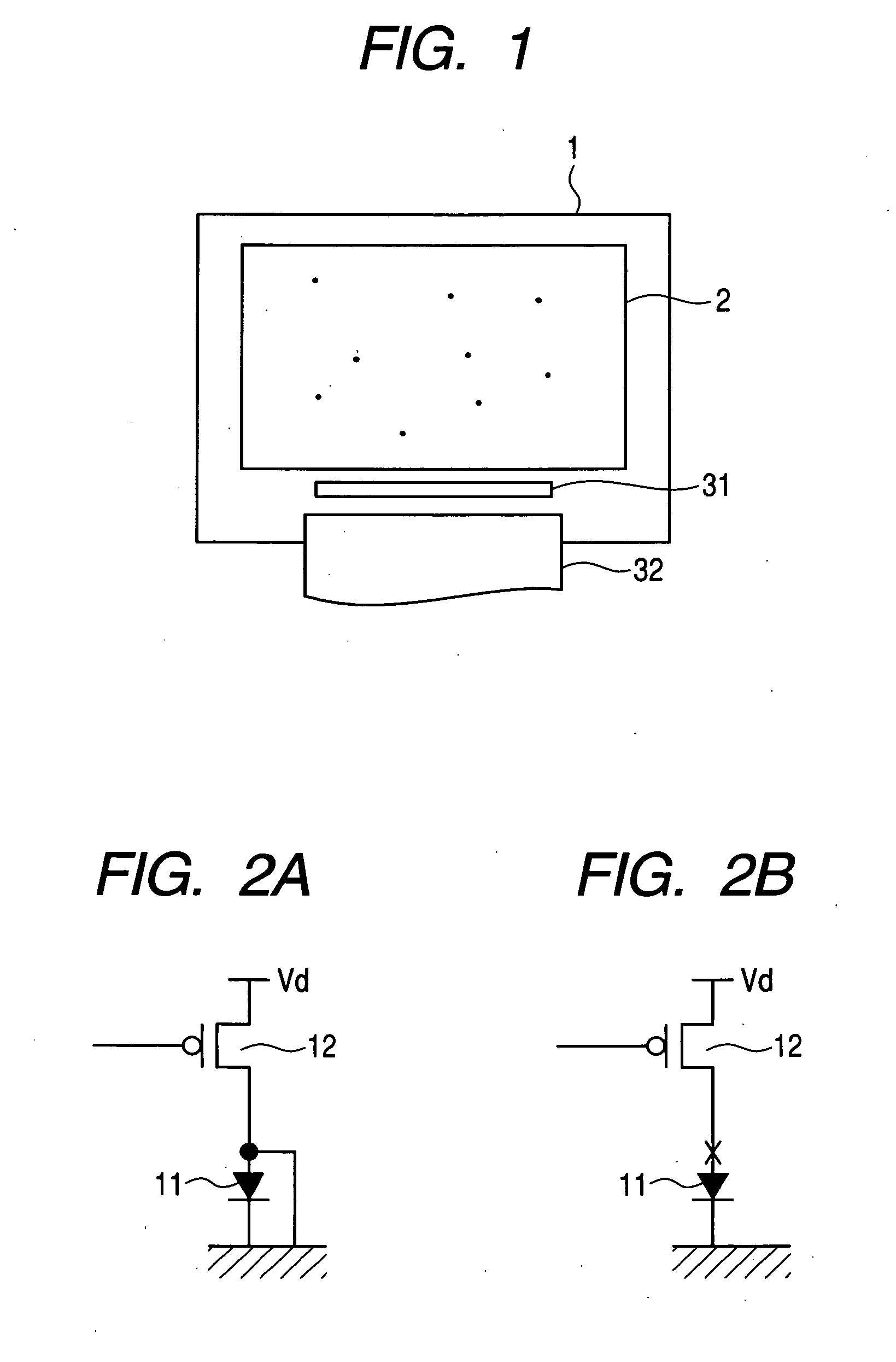
[0050]A large number of pixels PX are formed on the display area 2 shown in FIG. 1. All the pixels PX are not normal, and abnormal pixels exist as indicated by black points shown in FIG. 1. The aforementioned point denotes the portion where t...

second embodiment

[0079]In the first embodiment, the determination with respect to the burn-in of the pixel PX is made through the comparison between the pixel PX and the adjacent one. That is, the plate voltage of the OLED device 11 of the pixel to be measured is compared with that of the adjacent pixel. The aforementioned inspection, however, may cause the measurement error resulting from the comparison between the pixels to be accumulated.

[0080]In order to prevent the aforementioned error accumulation, the following process may be performed in the present embodiment. The organic electroluminescence display unit to which the present embodiment is applied has the same structure as the one shown in FIG. 10. The data of the respective pixels except those determined as being faulty by the failure determination unit 81 shown in FIG. 10 are transferred to the burn-in determination unit 82. In the present embodiment, the burn-in determination unit 82 generates the reference data serving as the reference o...

third embodiment

[0082]FIG. 13 shows an example of the organic electroluminescence display unit according to a third embodiment. In the embodiment, the process for detecting the data of the pixels PX on the detection line as the scanning line sequentially from the left as shown in FIG. 11 is the same as that of the first embodiment. In the present embodiment, the burn-in determination with respect to the pixel PX is performed through the comparison between the pixel PX and the data of the reference pixel rather than the comparison between the adjacent pixels.

[0083]In the embodiment, if the reference pixel is turned to be abnormal, all the correction data cannot be used. In order to overcome the aforementioned disadvantage, the reference pixel is also subjected to the periodic check whether or not it is maintained normal. For example, the normal range and the abnormal range for the reference data are predetermined as shown in FIG. 7. Then the process for eliminating the reference pixel determined as ...


PUM


Abstract

The voltage-current property of the specific pixel is measured to store the data on a single line in a line memory. The property data of adjacent pixels are compared. A failure determination unit detects whether or not the pixel to be compared is faulty. If it is determined as being faulty, the faulty pixel is removed from the pixel group to be compared. The burn-in determination unit performs the comparison using normal pixels only to provide the correct burn-in data. The calculation unit reflects the burn-in data in the image data from the host.

Description

CLAIM OF PRIORITY[0001]The present application claims priority from Japanese application JP 2007-057103 filed on Mar. 7, 2007, the content of which is hereby incorporated by reference into this application.FIELD OF THE INVENTION[0002]The present invention relates to an organic electroluminescence display, and more particularly to a display technique for correcting the change in the emission property of the organic electroluminescence device over operation time.BACKGROUND OF THE INVENTION[0003]Instead of the CRT which has been generally employed as the display, the demand for the use of the liquid crystal display, the plasma display and the like which has been put into practical use as the flat display has been increased. Furthermore, the display using the organic electroluminescence display (hereinafter referred to as OLED), and the display having electron sources using the field emission arranged in matrix for forming the image by allowing the fluorescent substance to emit on the a...

Claims


Application Information

Patent Timeline
Patent Type & Authority Applications(United States)
IPC IPC(8): G09G3/30
CPCG09G3/3233G09G2300/0809G09G2330/10G09G2320/046G09G2330/08G09G2320/0285
Inventor MIYAMOTO, MITSUHIDEKOHNO, TOHRUISHII, MASATOKASAI, NARUHIKOAKIMOTO, HAJIME
Owner JAPAN DISPLAY INC
Why Eureka
Try Eureka