Method of analyzing a wafer sample

a wafer sample and sample technology, applied in the field of methods of analyzing wafer samples, can solve the problems of inconsistent determination reference of analysis, affecting the quality of wafer samples, so as to facilitate the detection of weak points and easily set up the margin of an exposure process

Inactive Publication Date: 2008-09-11
SAMSUNG ELECTRONICS CO LTD
View PDF4 Cites 3 Cited by
  • Summary
  • Abstract
  • Description
  • Claims
  • Application Information

AI Technical Summary

Benefits of technology

[0020]According to example embodiments of the present invention, defects of a reference shot region and a shot region adjacent the reference shot region and defects of a shot region

Problems solved by technology

The determination reference, however, may unfortunately vary in accordance with the users.
Although the weak points of the photoresist pattern and the margin of the exposure process are analyzed by one user, a consistent determination reference of analysis may not be ensured because t

Method used


Image

  • Method of analyzing a wafer sample
  • Method of analyzing a wafer sample
  • Method of analyzing a wafer sample

Examples


Embodiment Construction

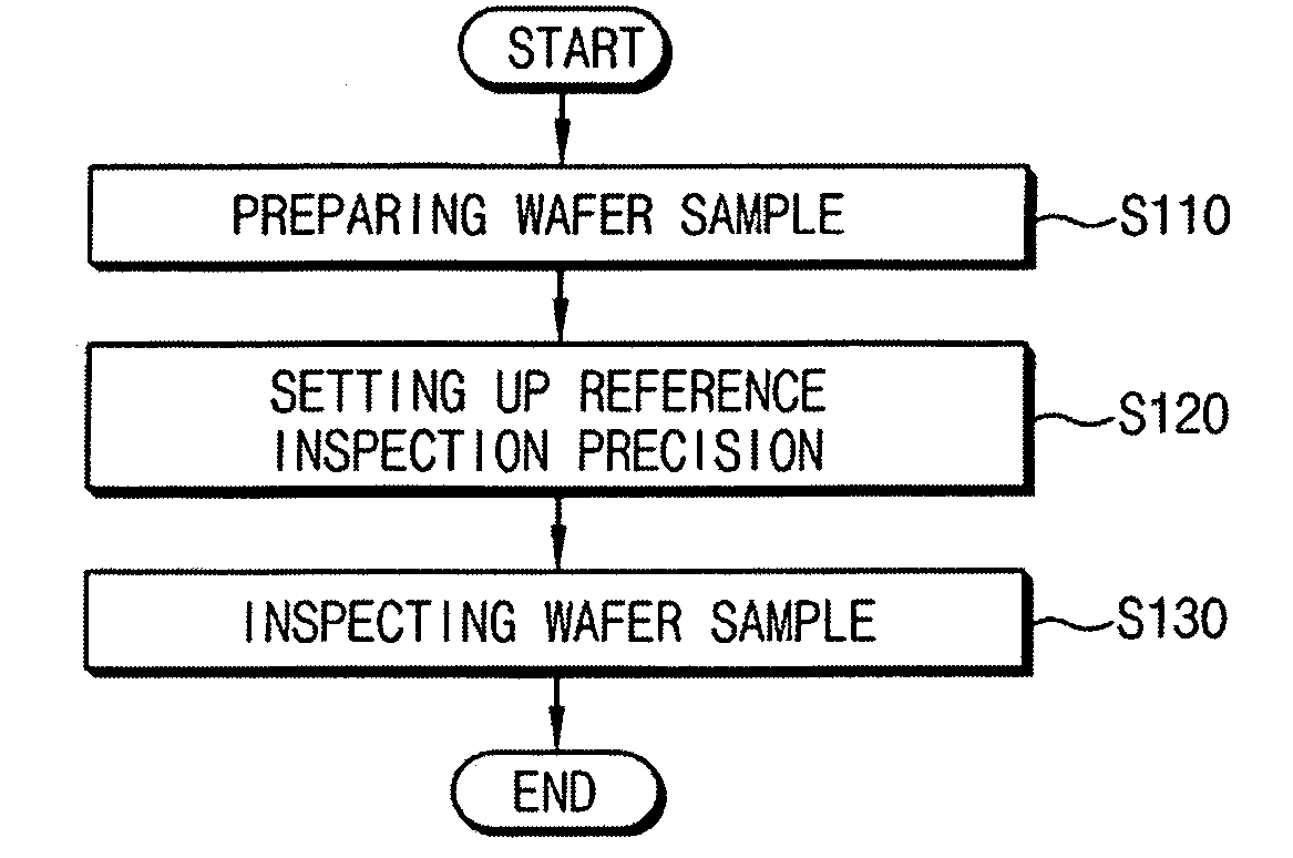
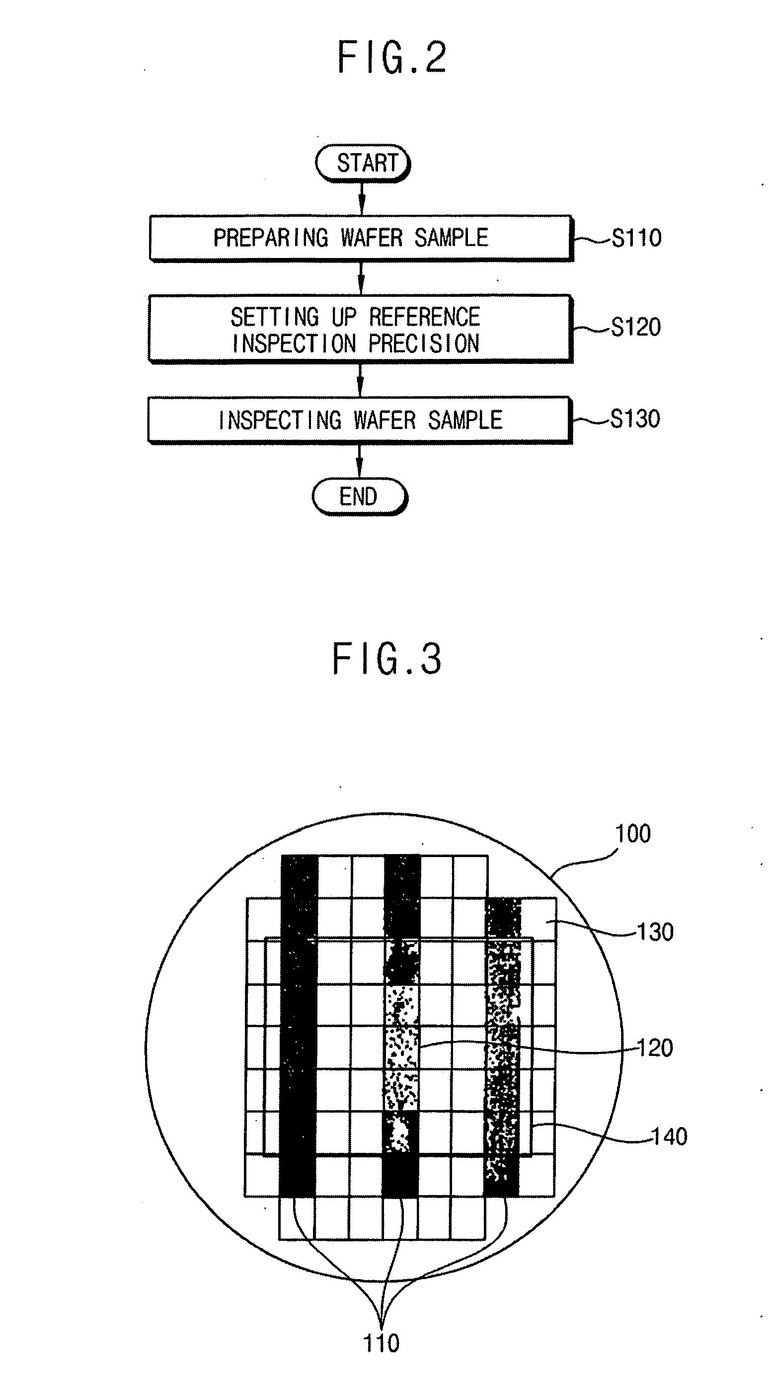
[0028]The present invention is described more fully hereinafter with reference to the accompanying drawings, in which example embodiments of the present invention are shown. The present invention may, however, be embodied in many different forms and should not be construed as limited to the example embodiments set forth herein. Rather, these example embodiments are provided so that this disclosure will be thorough and complete, and will fully convey the scope of the present invention to those of ordinary skill in the art.

[0029]It will be understood that, although the terms first, second, third etc. may be used herein to describe various elements, components, regions, layers and / or sections, these elements, components, regions, layers and / or sections should not be limited by these terms. These terms are only used to distinguish one element, component, region, layer or section from another region, layer or section. Thus, a first element, component, region, layer or section discussed b...


PUM


Abstract

In a method of analyzing a wafer sample, a first defect of a photoresist pattern on the wafer sample having shot regions exposed with related exposure conditions is detected. A first portion of the pattern includes the shot regions exposed with an exposure condition corresponding to a reference exposure condition and a tolerance error range of the reference exposure condition. The first defect repeatedly existing in at least two of the shot regions in a second portion of the pattern is set up as a second defect of the pattern. A first reference image displaying the second defect is obtained. The first defect of the shot regions in the first portion corresponding to the second defect is set up as a third defect corresponding to weak points of the pattern. The exposure conditions of the shot region having no weak points are set up as an exposure margin of an exposure process.

Description

CROSS-REFERENCE TO RELATED APPLICATION[0001]This application claims priority under 35 U.S.C. §119 to Korean Patent Application No. 2007-23253, filed on Mar. 9, 2007, the contents of which are herein incorporated by reference in their entireties.BACKGROUND OF THE INVENTION[0002]1. Technical Field[0003]Example embodiments of the present invention relate to a method of analyzing a wafer sample. More particularly, example embodiments of the present invention relate to a method of analyzing a wafer sample for detecting a weak point of a pattern in an exposure process to set up a desired margin of the exposure process.[0004]2. Discussion of Related Art[0005]Semiconductor devices are generally manufactured through repeatedly performing separate processes that include a deposition process for forming a layer on a substrate, a chemical mechanical polishing (CMP) process for planarizing the layer, a photo process for forming a photoresist pattern on the layer, an etching process for patternin...

Claims


Application Information

Patent Timeline
IPC IPC(8): G06K9/00
CPCG01N21/95607G06T2207/30148G06T2207/10061G06T7/001G03F7/7065H01L22/12
Inventor KIM, JONG-ANYANG, YU-SINJUN, CHUNG-SAMKANG, MOON-SHIKKIM, JI-HYE
Owner SAMSUNG ELECTRONICS CO LTD
Why Eureka
Try Eureka