Image forming apparatus and method of abrading photoconductor of the apparatus

Active Publication Date: 2008-09-11
KONICA MINOLTA BUSINESS TECH INC
View PDF2 Cites 2 Cited by
  • Summary
  • Abstract
  • Description
  • Claims
  • Application Information

AI Technical Summary

Benefits of technology

[0011]However, the aforementioned conventional techniques have the following disadvantages. The cleaning member can not fully remove the deposits from the photoconductor. After long use, therefore, the unremoved deposits will accumulate on the photoconductor and further increase in size, leading to image noises. A certain amount of deposits could be removed in the transfer section; however, the deposits may pass through the cleaning in a transfer destination and adhere again to the photoconductor as mentioned above.
[0012]When a speed difference is given between the photoconductor and the transfer body, removal of the deposits can be facilitated in the transfer section. However, a larger speed difference may deteriorate image quality. Increasing the amount of abrasive added in the developer will cause problems such as in-apparatus contamination and toner charging failure. Adding the abrading member will increase the complexity and size of the apparatus. The same applies to an apparatus configured to supply the abrasive to the cleaning member.
[0013]The present invention has been made in view of the above circumstances and has an object to provide an image forming apparatus and a method of abrading a photoconductor of the apparatus to allow appropriate refreshing of the photoconductor without excessively abrading the photoconductor to maintain good image quality over a long period.
[0014]To achieve the purpose of the invention, there is provided an image forming apparatus comprising a photoconductor, a toner image forming section for forming a toner image on the photoconductor, a contact member that is switchable between a contact state and a separate state with respect to the photoconductor so that the contact member contacts with the photoconductor during image formation period, and a non-image-formation-period control section that performs control to prevent contamination of a surface of the photoconductor during non image formation period, and is arranged to perform one of a first mode and a second mode, wherein the first mode being configured to hold the photoconductor and the contact member separate from each other during the non image formation period, and the second mode being configured to, during the non image formation period, perform an abrasion process for a predetermined time by rotating the photoconductor with a larger speed difference between the photoconductor and the contact member than that of the image formation period, while the photoconductor and the contact member are held in contact with each other, and hold the photoconductor and the contact member separate from each other for a period other than the abrasion process.
[0015]In the image forming apparatus of the present invention, accordingly, during non image formation period, either the first mode or the second mode is executed. In the first mode, the photoconductor and the contact member are held out of contact with each other to prevent back transfer of deposit matters from the contact member to the photoconductor. In the second mode, the abrasion process is performed within a predetermined time to remove the deposit matters from the photoconductor. Accordingly, the photoconductor can be refreshed and thus the image quality can be maintained.
[0019]According to the above configurations, the present invention can provide the image forming apparatus and the method of abrading the photoconductor, capable of refreshing the photoconductor appropriately without excessive abrasion thereof and maintaining good image quality for a long term.

Problems solved by technology

However, the aforementioned conventional techniques have the following disadvantages.
The cleaning member can not fully remove the deposits from the photoconductor.
After long use, therefore, the unremoved deposits will accumulate on the photoconductor and further increase in size, leading to image noises.
However, a larger speed difference may deteriorate image quality.
Increasing the amount of abrasive added in the developer will cause problems such as in-apparatus contamination and toner charging failure.
Adding the abrading member will increase the complexity and size of the apparatus.

Method used


Image

  • Image forming apparatus and method of abrading photoconductor of the apparatus
  • Image forming apparatus and method of abrading photoconductor of the apparatus
  • Image forming apparatus and method of abrading photoconductor of the apparatus

Examples


first example

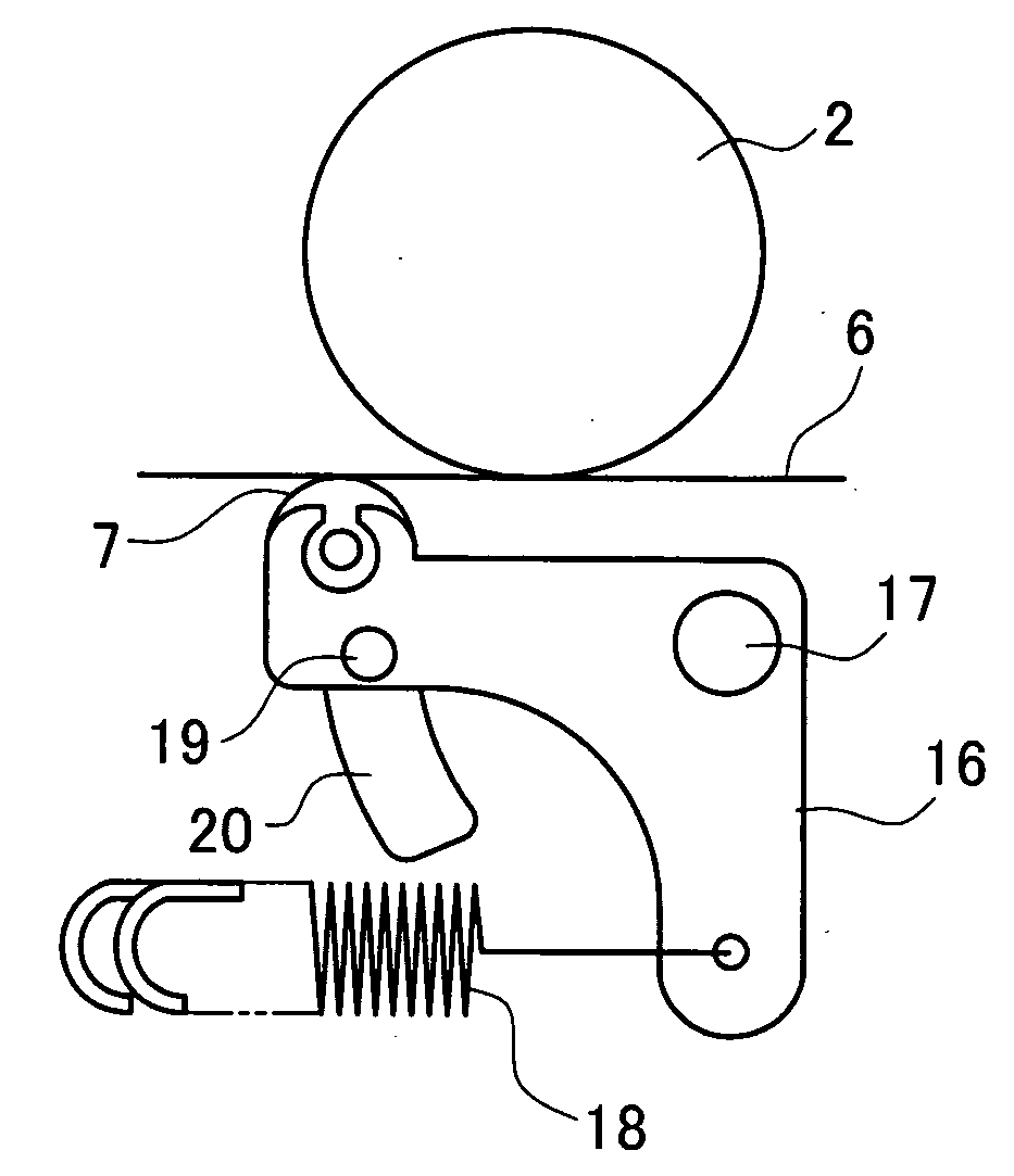
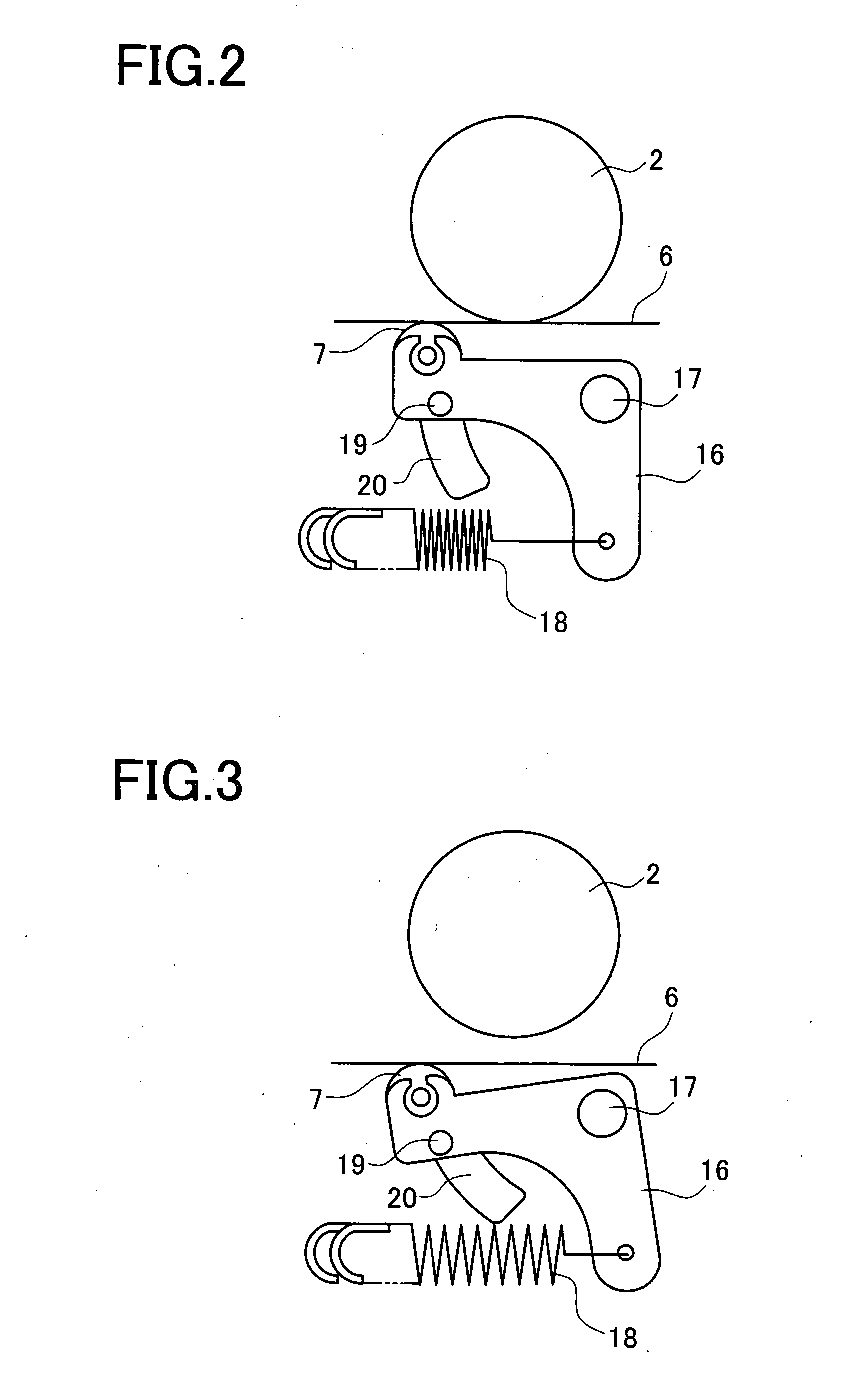
[0041]A first mode of a first example is explained below. In the first mode, each image forming unit 1 is controlled according to a timing chart shown in FIG. 5 after completion of image formation. In FIG. 5, a term “Photoconductor Contact” indicates a contact or separate condition between the photoconductive drum 2 and the intermediate transfer belt 6. “ON” represents a contact state (a state in FIG. 2) and “OFF” represents a separate state (a state in FIG. 3). This switching is of course based on movement of the aforementioned lever member 16.

[0042]A term “Photoconductor Speed” in FIG. 5 indicates the circumferential speed of the photoconductive drum 2 during rotation. A term “Transfer Speed” indicates the traveling speed of the intermediate transfer belt 6. A term “Secondary Transfer” indicates an ON / OFF state of bias voltage to the secondary transfer roller 8. Each of those parameters is also applied to timing charts shown in FIG. 6 and subsequent figures. As shown in FIG. 5, th...

second example

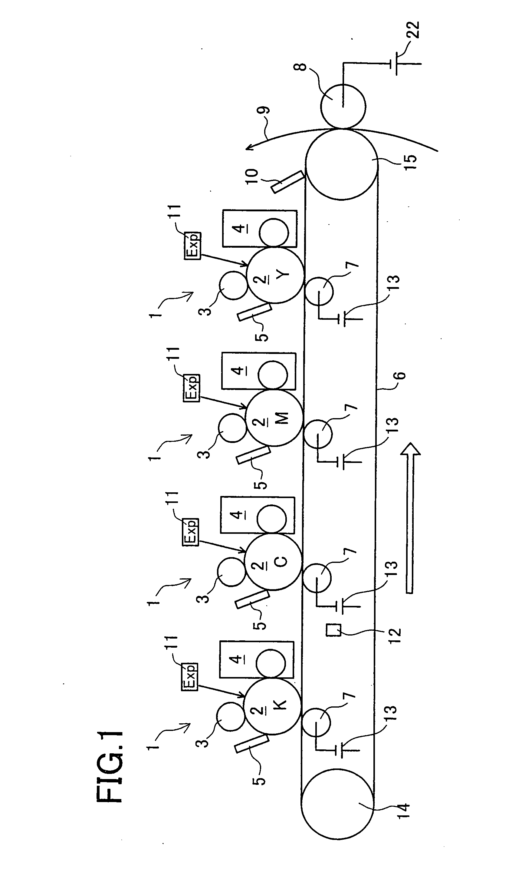
[0069]The aforementioned first example shows the abrasion of the photoconductive drum 2 to be performed only with the intermediate transfer belt 6. On the other hand, the second example shows the abrasion of the photoconductive drum 2 to be performed with the charge roller 3 in addition to the intermediate transfer belt 6.

[0070]FIG. 7 is a timing chart showing a process in the first mode of the second example to be performed after an end of image formation. In FIG. 7, “Charge Speed” indicates the circumferential speed of the charge roller 3 during rotation (the same applies to FIG. 8). Other conditions “Photoconductor Contact”, “Transfer Speed”, and “Secondary Transfer” are omitted from FIG. 7 for convenience of illustration but they are the same as those in FIG. 5. In this case, “Photoconductor Contact” represents only a contact state between the photoconductive drum 2 and the intermediate transfer belt 6. The photoconductive drum 2 and the charge roller 3 remain in contact with ea...


PUM


Abstract

An image forming apparatus of the present invention is arranged to hold an intermediate transfer belt and a photoconductive drum out of contact with each other. In a non image formation process in a first mode, the intermediate transfer belt and the photoconductive drum are separated from each other upon completion of the image formation, thereby preventing contamination of the photoconductive drum due to back transfer. In a non image formation process in a second mode, the intermediate transfer belt and the photoconductive drum are separated from each other upon completion of the image formation, and then the intermediate transfer belt and the photoconductive drum are contacted with each other again upon completion of secondary transfer of an image. They are driven for a predetermined time with a speed difference therebetween, thereby abrading the surface of the photoconductive drum to refresh it.

Description

CROSS-REFERENCE TO RELATED APPLICATIONS[0001]This application is based upon and claims the benefit of priority from the prior Japanese Patent Application No. 2007-059860 filed on Mar. 9, 2007, the entire contents of which are incorporated herein by reference.BACKGROUND OF THE INVENTION[0002]1. Field of the Invention[0003]The present invention relates to an electrophotographic image forming apparatus and, more particularly, to an image forming apparatus capable of preventing deterioration in image quality resulting from contamination of a photoconductor due to additive components to a developer, and a method of abrading the photoconductor.[0004]2. Description of Related Art[0005]As electrophotographic developers, heretofore, there are a two-component type developer containing toner and carrier and a single-component type developer containing no carrier. Many image forming apparatuses using such single-component type developer are provided with a friction member for helping frictional...

Claims


Application Information

Patent Timeline
IPC IPC(8): G03C1/765G03G15/00
CPCG03G15/752G03G15/0194G03G2215/0132
Inventor MATSUURA, KUNIYA
Owner KONICA MINOLTA BUSINESS TECH INC
Why Eureka
Try Eureka