
Flash memory system for improving read performance and read method thereof

a flash memory and read performance technology, applied in memory systems, redundancy data error correction, instruments, etc., can solve the problems of deteriorating program speed, affecting the performance of reads, and not easy for general users to update memory contents, so as to reduce the delay of data in memory controllers.

Inactive Publication Date: 2008-09-11
SAMSUNG ELECTRONICS CO LTD
View PDF17 Cites 72 Cited by
  • Summary
  • Abstract
  • Description
  • Claims
  • Application Information

AI Technical Summary

Benefits of technology

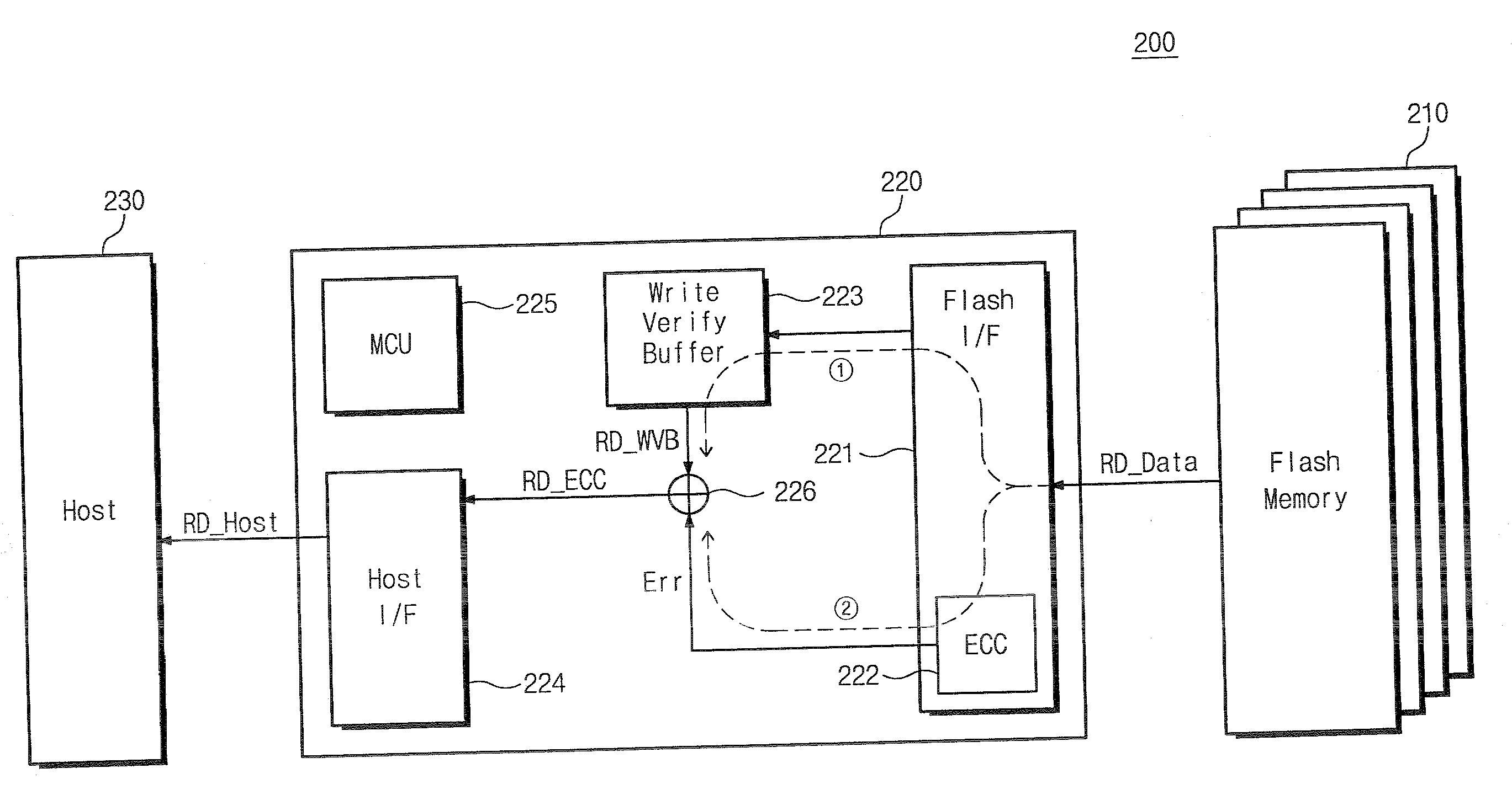
[0013]Exemplary embodiments of the present invention provide a data reading method and a device that minimize data delay in a memory controller including a low-performance error correction block.
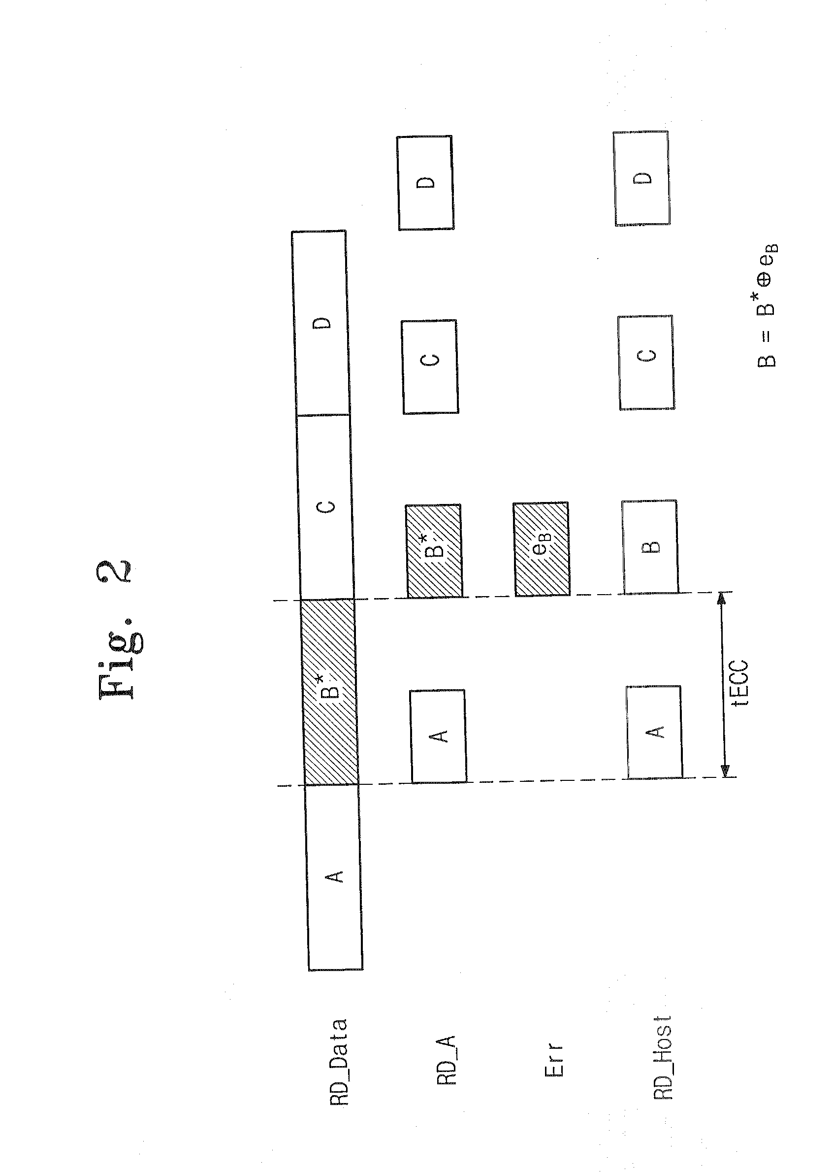
[0036]Exemplary embodiments provide an error correction time for generating the error vector of the error correction block that is longer than one clock during which time the buffer outputs the read data.

Problems solved by technology

In the MROM, PROM, and EPROM kinds of memories, it is not an easy task for a general user to update memory contents, because erase and write operations are not simple enough within a memory system itself.
This control method deteriorates a program speed, however, such that its efficiency decreases.
As more bits are stored in one memory cell, the error occurrence probability increases.
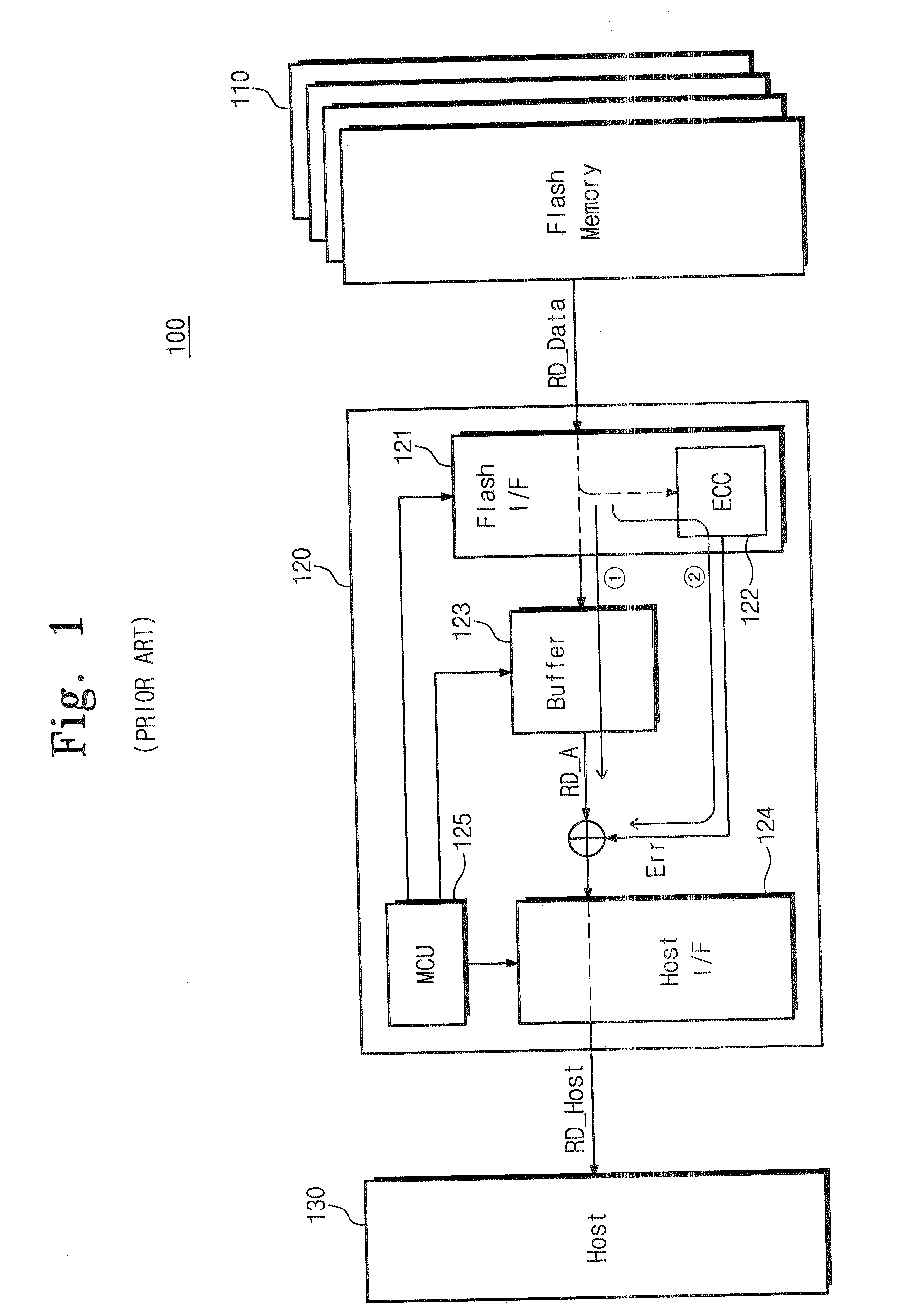
An error correction operation demands a relatively long time to correct the errors in the read data.
For the high-speed and high-performance error correction operation, an expensive, high-performance ECC block 122 is required.

Method used


Image

  • Flash memory system for improving read performance and read method thereof
  • Flash memory system for improving read performance and read method thereof
  • Flash memory system for improving read performance and read method thereof

Examples


Embodiment Construction

[0054]Exemplary embodiments of the present invention will be described below in more detail with reference to the accompanying drawings. The present invention may, however; be embodied in different forms and should not be constructed as limited to the exemplary embodiments set forth herein. Rather, these exemplary embodiments are provided so that this disclosure will be thorough and complete, and will fully convey the scope of the present invention to those skilled in the art. Like reference numerals refer to like elements throughout.

[0055]Hereinafter, a NAND type Hash memory device is used to explain features and functions of exemplary embodiments of the present invention. Those with ordinary skill in the art, however, easily understand other advantages and performance of the exemplary embodiments of the present invention according to the following descriptions. The present invention also can be embodied or applied through other exemplary embodiments. The above-disclosed subject ma...


PUM


Abstract

A method of transmitting data from a flash memory device to a host includes: detecting whether the data includes an error or not; performing an error correction operation for correcting the data having the error when the error exists in the data; and sequentially storing the data having the error and a plurality of subsequent read data without outputting. The storing of the data is performed during the performing of the error correction operation.

Description

CROSS-REFERENCE TO RELATED APPLICATION[0001]This patent application claims priority under 35 U.S.C. 119 of Korean Patent Application No. 2007-12822, filed on Feb. 7, 2007, the entire contents of which are hereby incorporated by reference.BACKGROUND OF THE INVENTION[0002]The present disclosure relates to a semiconductor memory device and, more particularly, to a read method of a non-volatile memory device.[0003]A semiconductor memory device is generally categorized as either a volatile or non-volatile memory device. Volatile memory devices are classified into dynamic random access memories (DRAMs) and static random, access memories (SRAMs). A volatile semiconductor device loses its stored data when a power supply is removed, while a non-volatile memory device retains its stored data even when no power supply is applied. Thus, non-volatile memories are widely used to store data in applications whose data retention is required regardless of the presence of a power supply. Examples of n...

Claims


Application Information

Patent Timeline
Patent Type & Authority Applications(United States)
IPC IPC(8): G11C29/00
CPCG11C2029/0411G06F11/1068G06F11/08G06F12/00G06F13/00
Inventor LEE, CHANG-DUCKHEO, SEOK-WONPARK, SI-YUNGLEE, DONG-RYOUL
Owner SAMSUNG ELECTRONICS CO LTD
Learn More