
System and method for inhibiting and containing resin bleed-out from adhesive materials used in assembly of semiconductor devices

a semiconductor device and resin technology, applied in the direction of semiconductor/solid-state device details, manufacturing tools, electrical apparatus construction details, etc., can solve the problems of ineffective metal strip for drastic bleed-out amounts, inability to prevent resin bleed-out through the bottom of the substrate, and defect that cannot be left on the device, etc., to achieve the effect of reducing lost production time and improving reliability and quality

Active Publication Date: 2008-09-18
TEXAS INSTR INC
View PDF8 Cites 7 Cited by
  • Summary
  • Abstract
  • Description
  • Claims
  • Application Information

AI Technical Summary

Benefits of technology

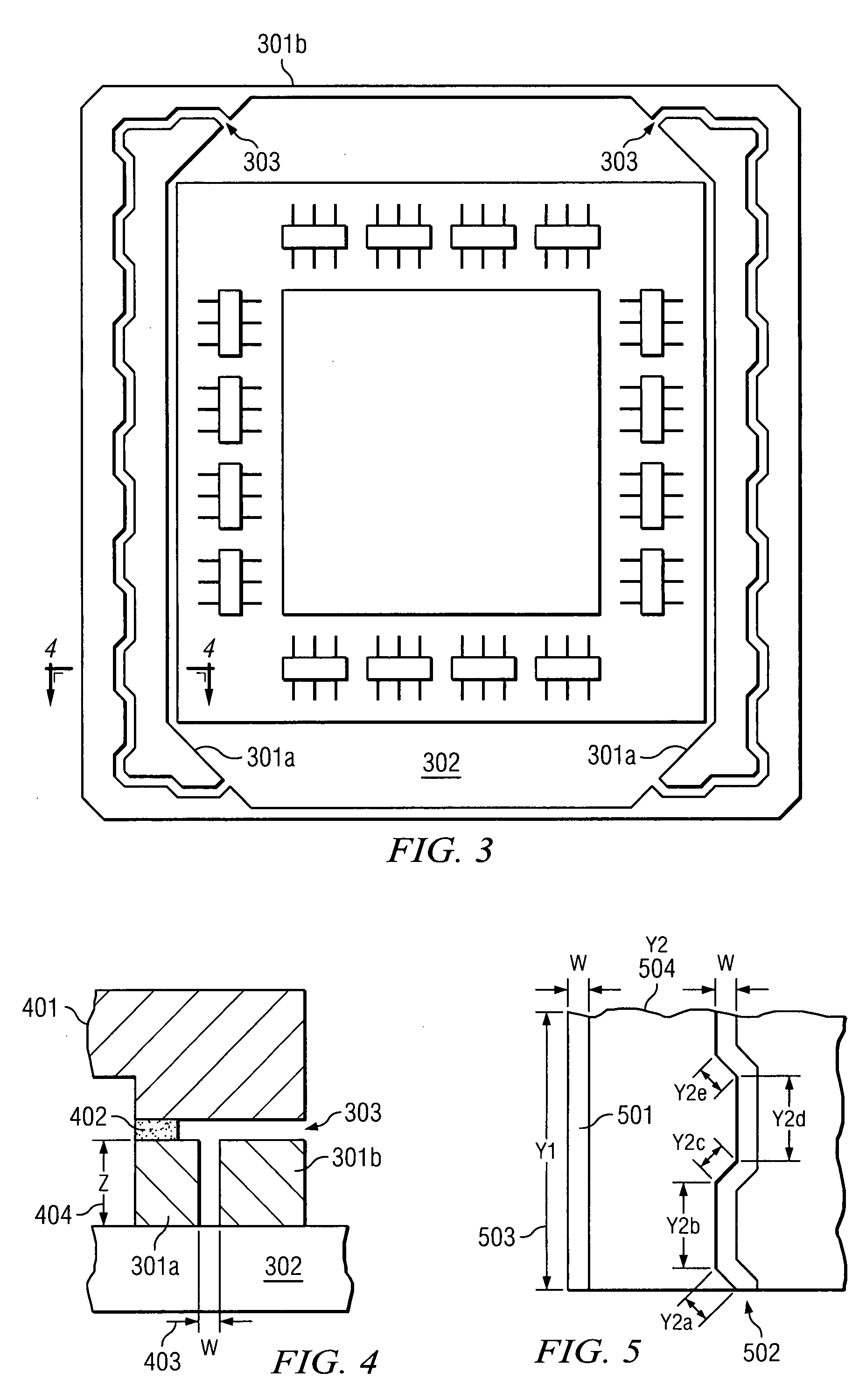
The present invention provides a method and device for assembling semiconductor devices using lid adhesive on gold surfaces. A trench or gap is formed between the first and second gold surfaces to act as a reservoir for resin bleed-out from the lid adhesive. This prevents resin bleed-out and contamination during flip chip assembly, improves reliability and quality, and reduces lost production time.

Problems solved by technology

This metal strip has proven to be ineffective for drastic bleed-out amounts.
Also, the metal strip does not prevent resin bleed-out through the bottom of the substrate.
This resin bleed out is a defect that cannot be left on the device after assembly.
One disadvantage of the prior art is the loss in manufacturing time caused by the need to clean the resin bleed-out from the package.
Detecting and cleaning resin bleed-out cause production delays and requires extra personnel, which adds to the cost of production.
A second disadvantage caused by resin bleed-out is potential contamination of the test board used to test the completed devices.
If resin bleed-out remains on the LGA pads and the device is placed in a socket on a test board, the resin is likely to transfer to the test socket, which, in turn, could also contaminate all subsequently tested devices.

Method used


Image

  • System and method for inhibiting and containing resin bleed-out from adhesive materials used in assembly of semiconductor devices
  • System and method for inhibiting and containing resin bleed-out from adhesive materials used in assembly of semiconductor devices
  • System and method for inhibiting and containing resin bleed-out from adhesive materials used in assembly of semiconductor devices

Examples


Embodiment Construction

[0019]The making and using of the presently preferred embodiments are discussed in detail below. It should be appreciated, however, that the present invention provides many applicable inventive concepts that can be embodied in a wide variety of specific contexts. The specific embodiments discussed are merely illustrative of specific ways to make and use the invention, and do not limit the scope of the invention.

[0020]The present invention will be described with respect to preferred embodiments in a specific context, namely the manufacture of flip chip semiconductor microprocessors. The invention may also be applied, however, to any flip chip assembly or other device in which resin-based adhesive is used on a ceramic or porous substrate.

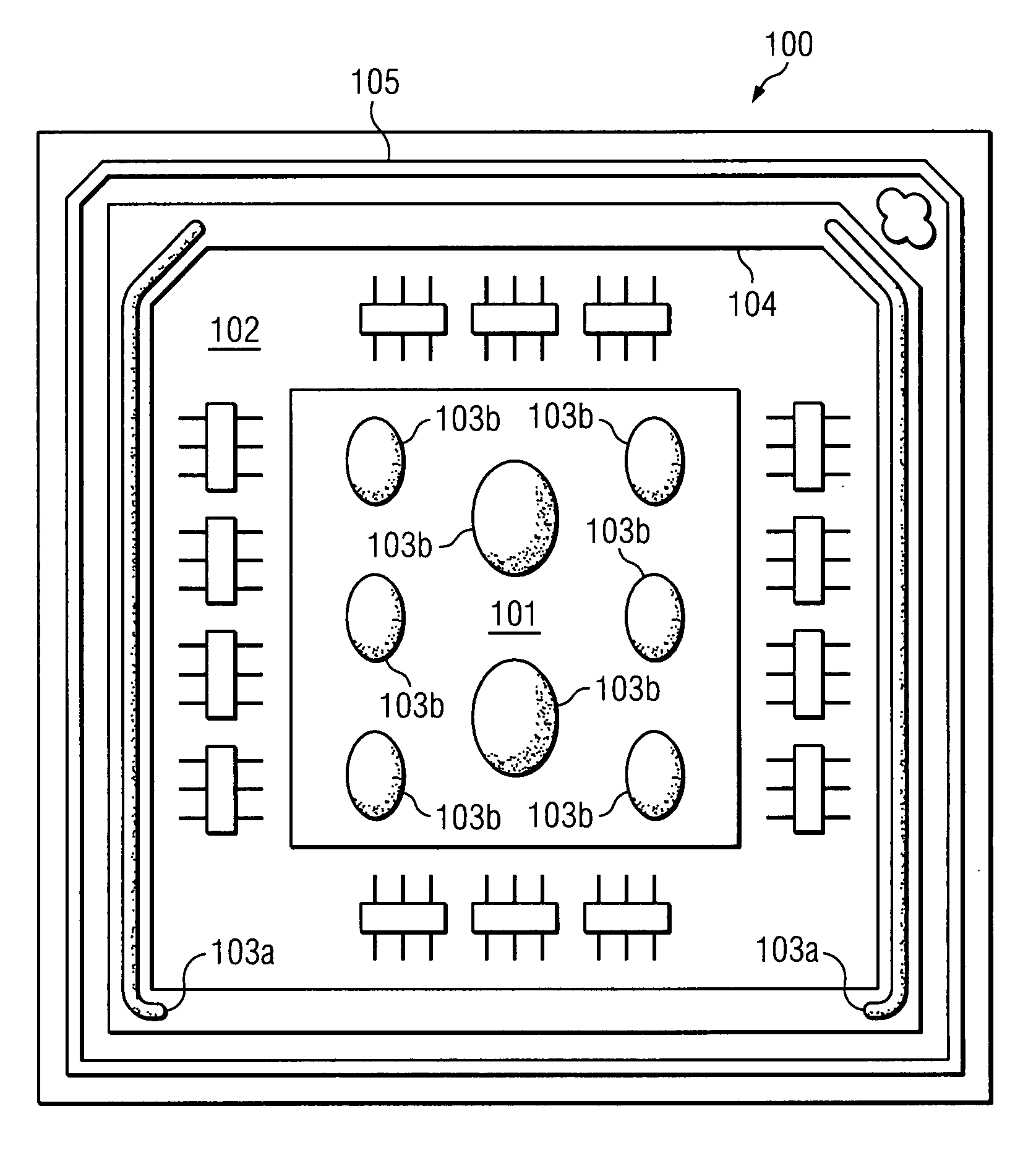
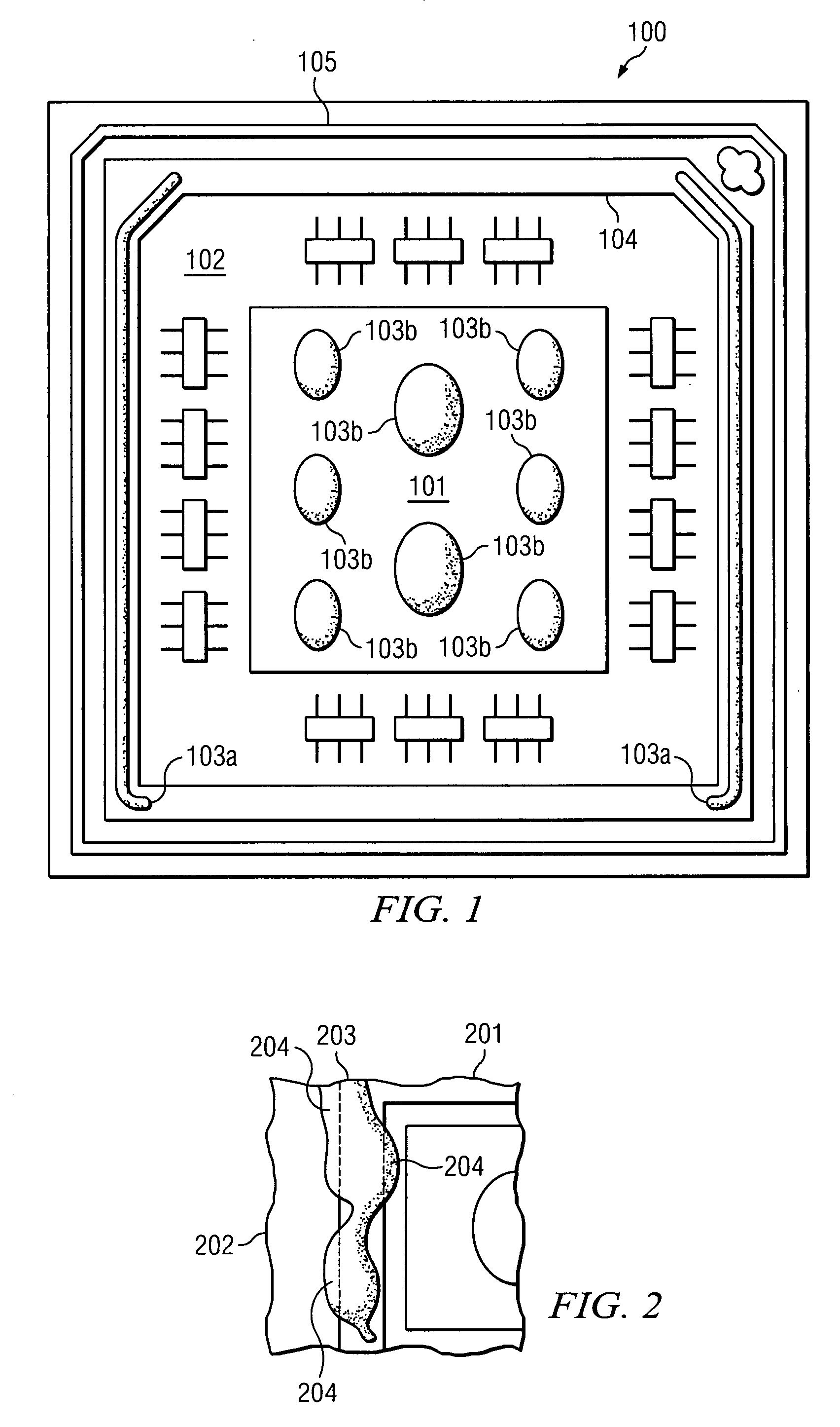
[0021]FIG. 1 is an exemplary embodiment of the present invention in which device 100 comprises die 101 bonded to substrate 102. Lid adhesive 103a and 103b has been applied to device 100; however, instead of being applied directly to substrate 102, adh...


PUM

PropertyMeasurementUnit
shapeaaaaaaaaaa
widthaaaaaaaaaa
surface roughnessaaaaaaaaaa

Abstract

System and method for preventing resin-based adhesive from contacting a substrate to minimize resin bleed-out and contamination. A preferred embodiment comprises a semiconductor device having a die mounted on a substrate, first and second gold surfaces formed on the substrate, a trench formed between the first and second gold surfaces, resin-based adhesive applied to the first gold surface, and a heat sink bonded to the resin-based adhesive.

Description

TECHNICAL FIELD[0001]The present invention relates generally to a system and method for containing resin that bleeds out of adhesive and, more particularly, to a system and method for preventing resin bleed-out from contaminating semiconductor devices.BACKGROUND[0002]During flip chip semiconductor device assembly, a die, such as a microprocessor, is mounted on a substrate. A heat sink lid is then attached on top of the die and the substrate using a lid adhesive. The lid adhesive may be any commercially available adhesive, such as Lord MT-315 resin-based lid adhesive. The lid adhesive is applied in a predetermined dispense pattern in which some lid adhesive is applied to the substrate and other lid adhesive is applied to the die. It has been observed that when the lid adhesive is applied to the substrate, resin bleeds out of the lid adhesive and flows through to the bottom side of the substrate.[0003]Dispensing resin-based lid adhesive directly over a ceramic substrate accelerates re...

Claims


Application Information

Patent Timeline
Patent Type & Authority Applications(United States)
IPC IPC(8): H05K7/20B21D39/03
CPCH01L23/10H01L2924/01079Y10T29/49826H01L2924/0002H01L2924/00
Inventor MARTINEZ, SERGIO V.LEE, BOON HORROBINSON, KAREN LYNNE
Owner TEXAS INSTR INC
Learn More