Light emitting diode

a diode and light-emitting technology, applied in the direction of basic electric elements, electrical equipment, semiconductor devices, etc., can solve the problems of limiting the current distribution, unable to uniformly distribute the current, and not continuously emitting ligh

Active Publication Date: 2008-09-25
SEOUL VIOSYS CO LTD
View PDF10 Cites 130 Cited by
  • Summary
  • Abstract
  • Description
  • Claims
  • Application Information

AI Technical Summary

Benefits of technology

[0012]An object of the present invention is to provide an AC LED having an electrode structure in which a current flowing in operation of the LED can be uniformly distributed and the light efficiency can be enhanced.
[0013]According to an aspect of the present invention for achieving the objects, there is provided an AC LED, which comprises a substrate, and at least one serial array having a plurality of light emitting cells connected in series on the substrate. Each of the light emitting cells comprises a lower semiconductor layer consisting of a first conductive compound semiconductor layer formed on top of the substrate, an upper semiconductor layer consisting of a second conductive compound semiconductor layer formed on top of the lower semiconductor layer, an active layer interposed between the lower and upper semiconductor layers, a lower electrode formed on the lower semiconductor layer exposed at a first corner of the substrate, an upper electrode layer formed on the upper semiconductor layer, and an upper electrode pad formed on the upper electrode layer exposed at a second corner of the substrate. The upper electrode pad and the lower electrode are respectively disposed at the corners diagonally opposite to each other; and the respective light emitting cells are arranged so that the upper electrode pad and the lower electrode of one of the light emitting cells are symmetric with respect to those of adjacent another of the light emitting cells.

Problems solved by technology

As a result, there are problems in that the LED does not continuously emit light and is easily broken by reverse current.
Since the P-type semiconductor layer generally has high specific resistivity, there is a problem in that the current cannot be uniformly distributed but is concentrated on a portion at which the P-type electrode is formed.
However, since the transparent electrode layer absorbs light, the thickness of the transparent electrode is restricted, and therefore, there is a limit in the current distribution.

Method used


Image

  • Light emitting diode
  • Light emitting diode
  • Light emitting diode

Examples


Embodiment Construction

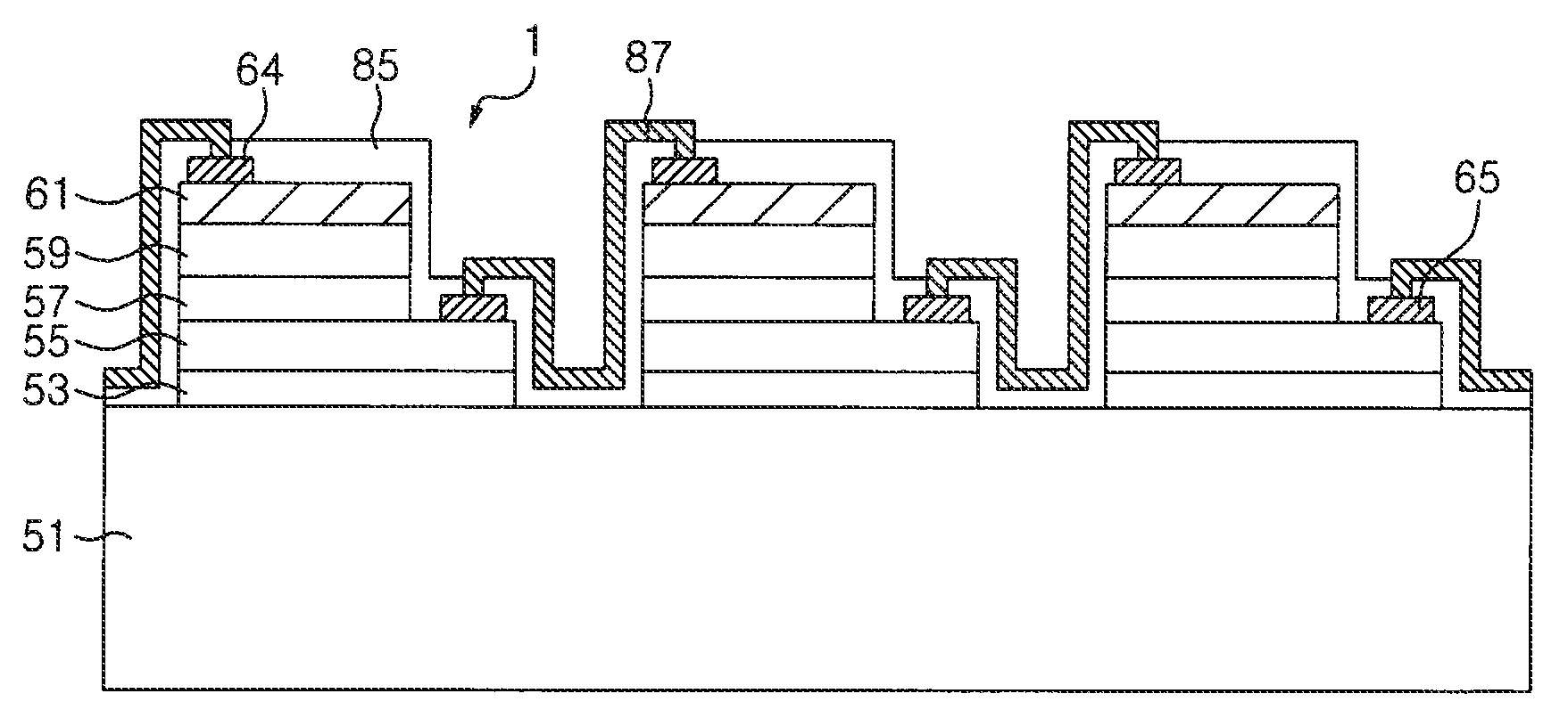
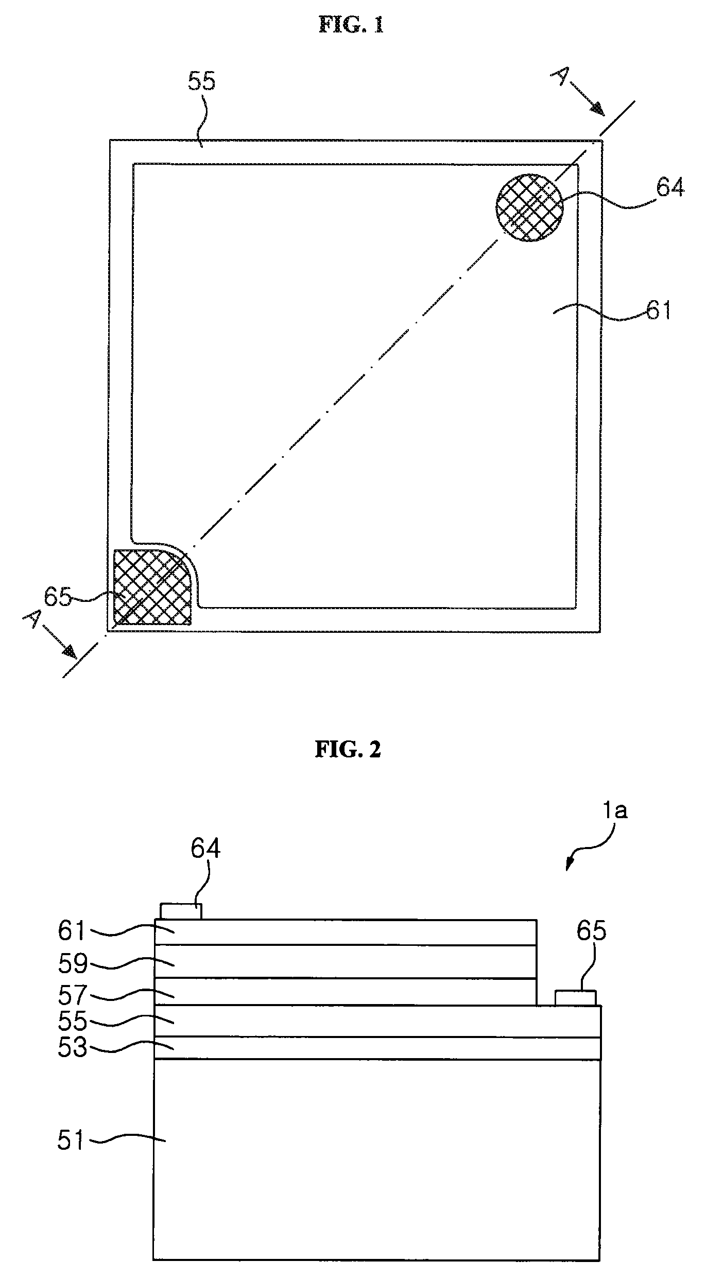
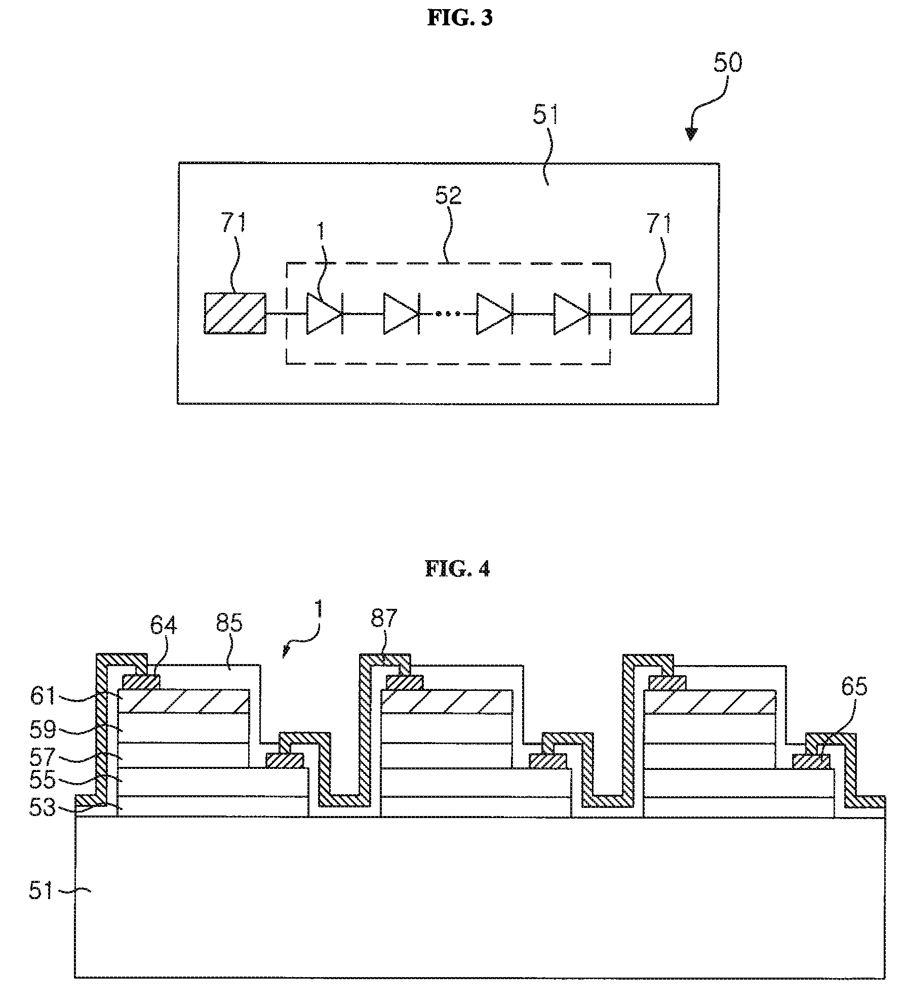
[0038]Hereinafter, preferred embodiments of the present invention will be described in detail with reference to the accompanying drawings. The following embodiments are provided only for illustrative purposes so that those skilled in the art can fully understand the spirit of the present invention. Therefore, the present invention is not limited to the following embodiments but may be implemented in other forms. In the drawings, the widths, lengths, thicknesses and the like of elements may be exaggerated for convenience of illustration. Like reference numerals indicate like elements throughout the specification and drawings.

[0039]FIG. 1 is a plan view illustrating an LED having a single light emitting cell with an electrode structure according to one embodiment of the present invention, and FIG. 2 is a sectional view taken along line A-A of FIG. 1. The technical structures and characteristics, which are used in describing the LED having a single light emitting cell with an electrode...


PUM


Abstract

AC LED according to the present invention comprises a substrate, and at least one serial array having a plurality of light emitting cells connected in series on the substrate. Each of the light emitting cells comprises a lower semiconductor layer consisting of a first conductive compound semiconductor layer formed on top of the substrate, an upper semiconductor layer consisting of a second conductive compound semiconductor layer formed on top of the lower semiconductor layer, an active layer interposed between the lower and upper semiconductor layers, a lower electrode formed on the lower semiconductor layer exposed at a first corner of the substrate, an upper electrode layer formed on the upper semiconductor layer, and an upper electrode pad formed on the upper electrode layer exposed at a second corner of the substrate. The upper electrode pad and the lower electrode are respectively disposed at the corners diagonally opposite to each other, and the respective light emitting cells are arranged so that the upper electrode pad and the lower electrode of one of the light emitting cells are symmetric with respect to those of adjacent another of the light emitting cells.

Description

RELATED APPLICATIONS[0001]This application claims priority of Korean Application NO. 10-2007-0026697, filed Mar. 19, 2007, the contents of which are incorporated herein by reference in their entirety.FIELD OF THE INVENTION[0002]The present invention relates to a light emitting diode, and more particularly, to a light emitting diode, wherein a region of the light emitting diode occupied by an upper electrode pad and a lower electrode is designed to be small to thereby reduce a region where light emitted from the light emitting diode is blocked by the upper electrode pad and the lower electrode and secure a larger light emitting area, thereby improving light emission efficiency.BACKGROUND OF THE INVENTION[0003]GaN-based light emitting diodes (LEDs) have been employed and developed for about 10 years or more. The GaN-based LEDs considerably have changed LED technologies and are currently used for various applications, such as full-color LED display devices, LED traffic lights and white...

Claims


Application Information

Patent Timeline
Patent Type & Authority Applications(United States)
IPC IPC(8): H01L33/00H01L33/06H01L33/08H01L33/32H01L33/38H01L33/42H01L33/62
CPCH01L27/156H01L33/385H01L33/62H01L27/15H01L2924/0002H01L2924/00H01L33/387
Inventor YOON, YEO JINKIM, JONG KYULEE, JUN HEE
Owner SEOUL VIOSYS CO LTD
Why Eureka
Try Eureka