Coupled inductor structure
- Summary
- Abstract
- Description
- Claims
- Application Information
AI Technical Summary
Benefits of technology
Problems solved by technology
Method used
Image

Examples
first embodiment
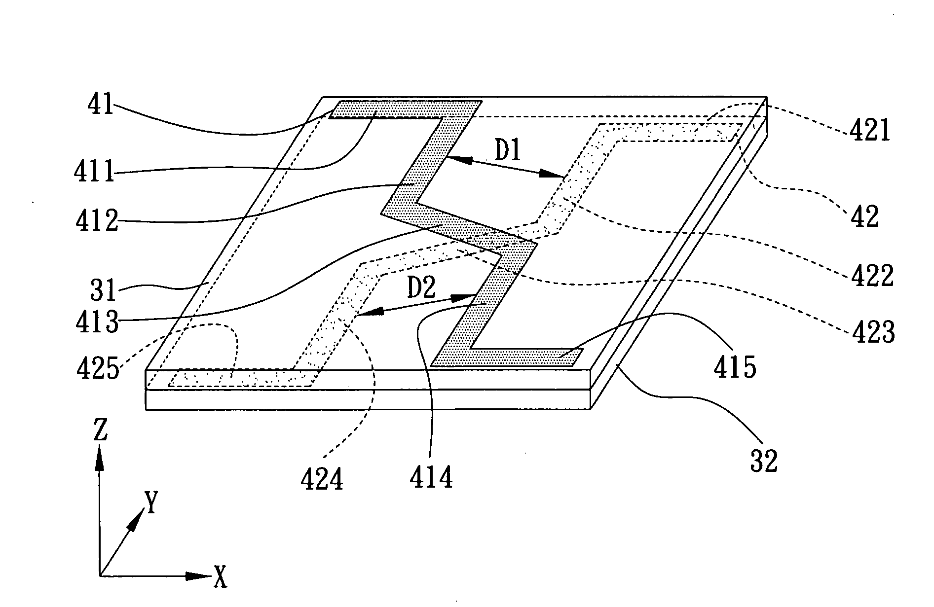
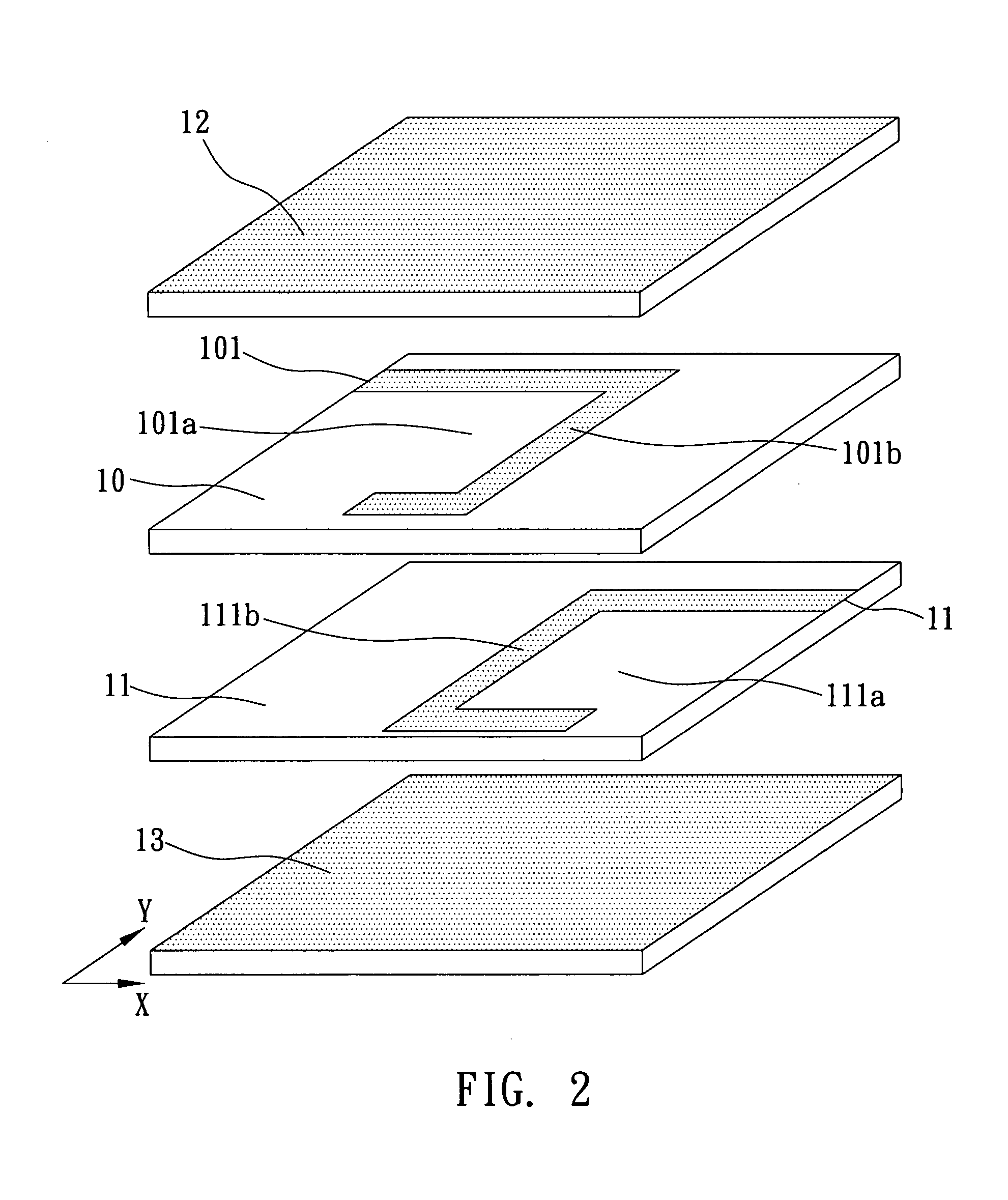
[0023]With reference to FIG. 3a, an exploded view of a coupled inductor structure according to a first embodiment of the present invention is shown. As shown in the drawing, the coupled inductor structure is applied in a plurality of dielectric layers 3 comprising at least one first dielectric layer 31 and one second dielectric layer 32 disposed under the first dielectric layer 31 and having an electrically conductive through hole 321.
[0024]The coupled inductor structure according to the present invention comprises a first inductor element 41 disposed on the first dielectric layer 31 and a second inductor element 42 disposed on the second dielectric layer 32. It is appreciated to those skilled in the art that variation in the quantity of the inductor elements, the first inductor element 41 and / or the second inductor element 42, is easily accomplished without departing from the spirit of the present invention and involves only routine practice in the field such that the change in num...
second embodiment
[0038]With reference to FIGS. 4a and 4b, a coupled inductor structure according to another embodiment of the present invention is shown. As shown in the drawings, the structure of the present embodiment is substantially same as the first embodiment. The only difference between them is that the first inductor element 41 further comprises a fourth bending segment 416 and a fifth bending segment 417 disposed between the third bending segment 414 and the second signal connecting port 415, wherein the fourth bending segment 416 is connected to the third bending segment 414, and the fifth bending segment 417 is connected to the fourth bending segment 416 and the second signal connecting port 415; and the second inductor element 42 further comprises a fourth bending segment 426 and a fifth bending segment 427 disposed between the third bending segment 424 and the second signal connecting port 425, wherein the fourth bending segment 426 is connected to the third bending segment 424, and the...
PUM
 Abstract
Description
Claims
Application Information
 - R&D Engineer
- R&D Manager
- IP Professional
- Industry Leading Data Capabilities
- Powerful AI technology
- Patent DNA Extraction
Browse by: Latest US Patents, China's latest patents, Technical Efficacy Thesaurus, Application Domain, Technology Topic.
© 2024 PatSnap. All rights reserved.Legal|Privacy policy|Modern Slavery Act Transparency Statement|Sitemap