Amplifier switching control circuit and method for current shunt instrumentation amplifier having extended position and negative input common mode range

a technology of amplifier switching control and amplifier, which is applied in the direction of amplifier details, differential amplifiers, amplifiers with semiconductor devices/discharge tubes, etc., can solve the problems of undesirable “glitches” of positive common mode voltage instrumentation amplifiers

Active Publication Date: 2007-03-27
TEXAS INSTR INC
View PDF3 Cites 15 Cited by
  • Summary
  • Abstract
  • Description
  • Claims
  • Application Information

AI Technical Summary

Benefits of technology

[0010]It is an object of the present invention to provide an instrumentation amplifier which has a wide common mode input voltage range in order to effectively reject both positive and negative transient voltage spikes.
[0012]It is another object of the invention to provide an instrumentation amplifier which has a wide common mode input voltage range and which avoids producing abrupt changes and / or inaccuracies in its output signal if the common mode input voltage applied to the instrumentation amplifier undergoes a transition from a positive to a negative value or vice versa.
[0013]Briefly described, and in accordance with one embodiment, the present invention provides an amplifier circuit including first (7A) and second (7B) operational amplifiers connected in a generally parallel configuration, each with inputs coupled through the same pair of matched input resistors which receive a differential input signal that may have both a positive and negative common mode range. An offset adjustment amplifier (17) receives a differential error signal representative of the difference between offset voltages of the first and second operational amplifiers and generates offset adjustment signals that are applied to the input stage of at least one of the first and second operational amplifiers to adjust their respective offset voltages so as to equalize them. With the offset voltages equalized, the first and second operational amplifiers operate seamlessly as a common mode component of the differential input signal undergoes a transition from its positive to its negative range, so as to avoid inaccuracies and abrupt changes in an output voltage during the transition , the output voltage being produced by the first and second operational amplifiers.
[0014]In the described embodiments, an instrumentation amplifier circuit (100) including a first operational amplifier (7A) having a non-inverting input coupled to a first terminal of a first input resistor (5), an inverting input coupled to a first terminal of a second input resistor (6), and an output (10A) coupled to a control electrode (e.g., base) of a first output transistor (Q1). The first output transistor (Q1) has a first electrode (e.g., emitter) coupled to a first output conductor (11AB) and a first terminal of a load resistor (RL) and a second electrode (e.g., collector) coupled to the first terminal of the first resistor (5), the load resistor (RL) having a second terminal coupled to a first reference voltage (GND). A differential input voltage is applied between a second terminal (2) of the first input resistor (5) and a second terminal (3) of the second input resistor (6). The differential input voltage has a common mode component that extends through both a positive and negative voltage range. The instrumentation amplifier also includes a second operational amplifier (7B) having an inverting input coupled to the first terminal of the first resistor (5), a non-inverting input coupled to the first terminal of the second resistor (6), and an output (10B) coupled to a control electrode (e.g., base) of a second output transistor (Q2) and a control electrode (e.g., base) of a level translation transistor (Q3), the second output transistor (Q2) having a first electrode (e.g., emitter) coupled to a second reference voltage (V+) and a second electrode (e.g., collector) coupled to the first terminal of the second resistor (6), the level translation transistor (Q3) having a first electrode (e.g., emitter) coupled to the second reference voltage (V+) and a second electrode (e.g., collector) coupled to the first output conductor (11AB). The instrumentation amplifier further includes offset adjustment circuitry including an offset control amplifier (17) having a non-inverting input and an inverting input for receiving a differential error signal representative of a difference between an offset voltage of the first operational amplifier (7A) and an offset voltage of the second operational amplifier (7B). A first transistor (Q5) has a control electrode (e.g., base) coupled to the output (10A) of the first operational amplifier (7A), a first electrode (e.g., emitter) coupled to the non-inverting input of the offset control amplifier (17), and a second electrode (collector) coupled to the second reference voltage (V+). A second transistor (Q4) has a control electrode (e.g., base) coupled to the output (10B) of the second operational amplifier (7B), a first electrode (e.g., emitter) coupled to the second reference voltage (V+), and a second electrode (collector) coupled to the inverting input of the offset control amplifier (17). The offset control amplifier (17) includes a first offset adjustment output (23-1,2) operatively coupled to adjust an offset voltage of one of the first (7A) and (7A) operational amplifiers. The offset adjustment circuitry operates so as to minimize a difference between offset voltages of the first (7A) and second (7B) operational amplifiers.
[0018]In a described embodiment, the offset control amplifier (17) is operatively coupled to the first (7A) and second (7B) operational amplifiers so as to cause one of them to dominate the other within a transition region between positive and negative values of a common mode component of the differential input voltage in order to prevent abrupt and / or indeterminate values of an output voltage produced on the first output conductor (11AB) within the transition region.

Problems solved by technology

However, in such applications, positive common mode voltage instrumentation amplifier1 may produce undesirable “glitches” in the output voltage Vout.

Method used


Image

  • Amplifier switching control circuit and method for current shunt instrumentation amplifier having extended position and negative input common mode range
  • Amplifier switching control circuit and method for current shunt instrumentation amplifier having extended position and negative input common mode range
  • Amplifier switching control circuit and method for current shunt instrumentation amplifier having extended position and negative input common mode range

Examples


Embodiment Construction

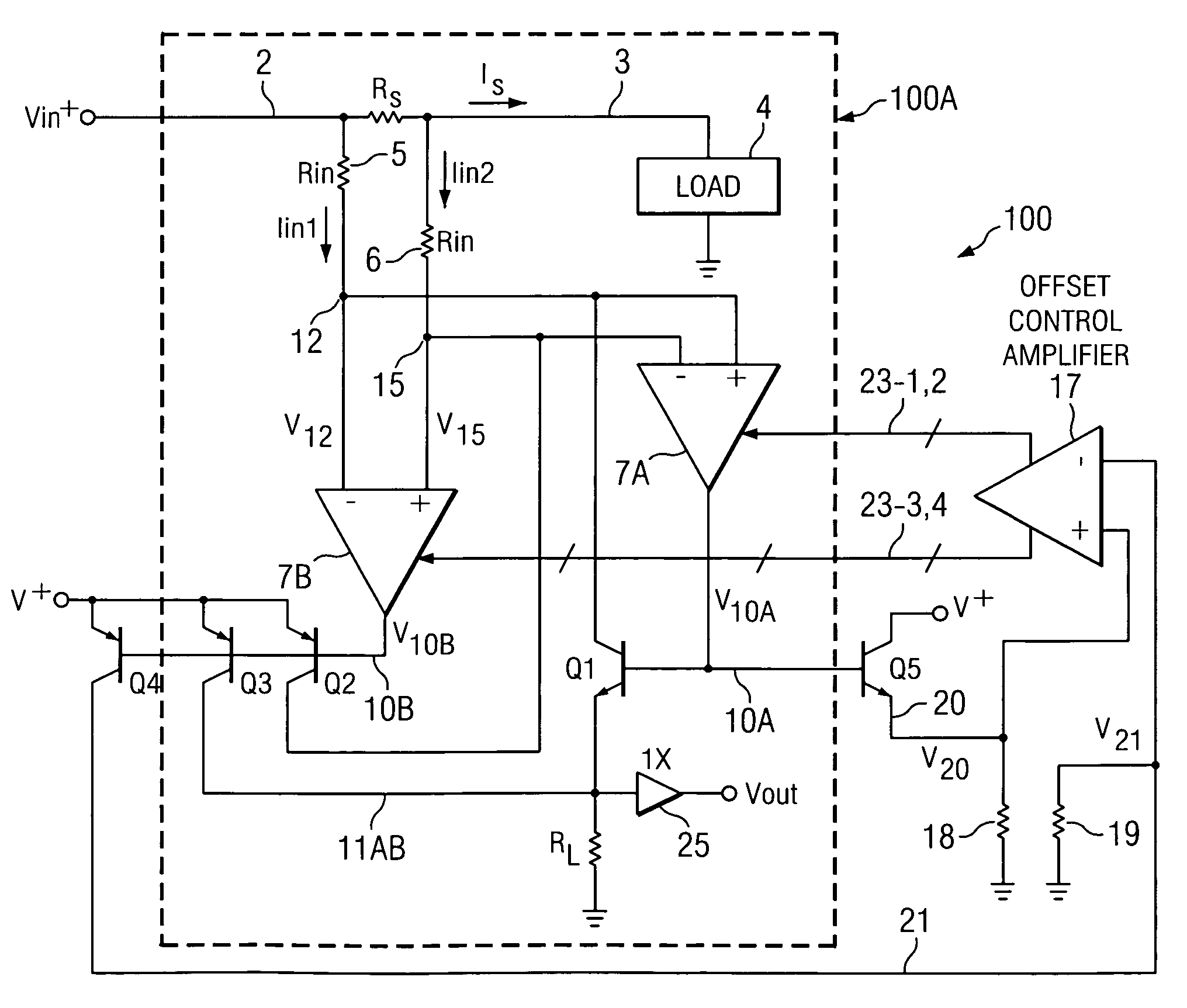
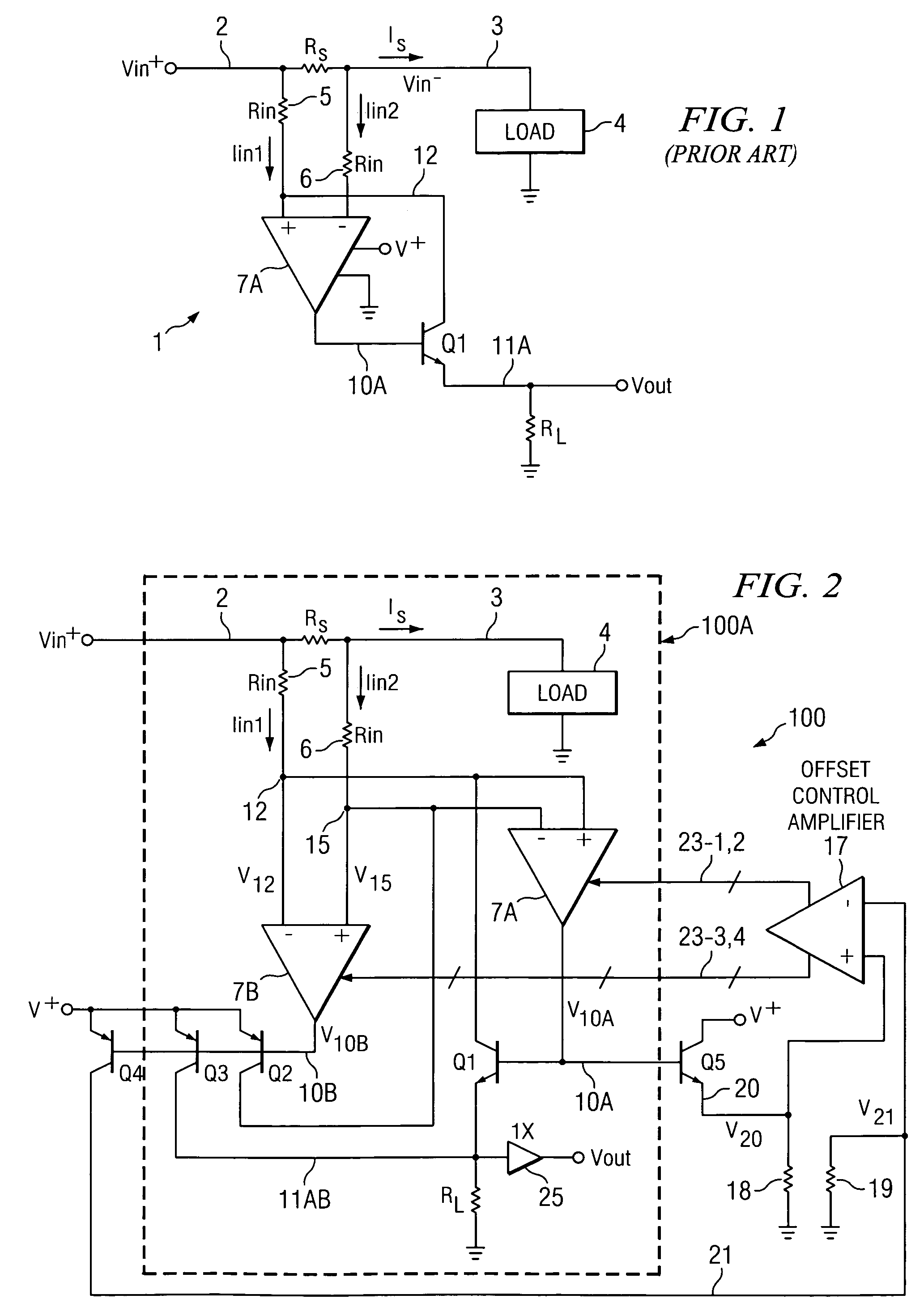
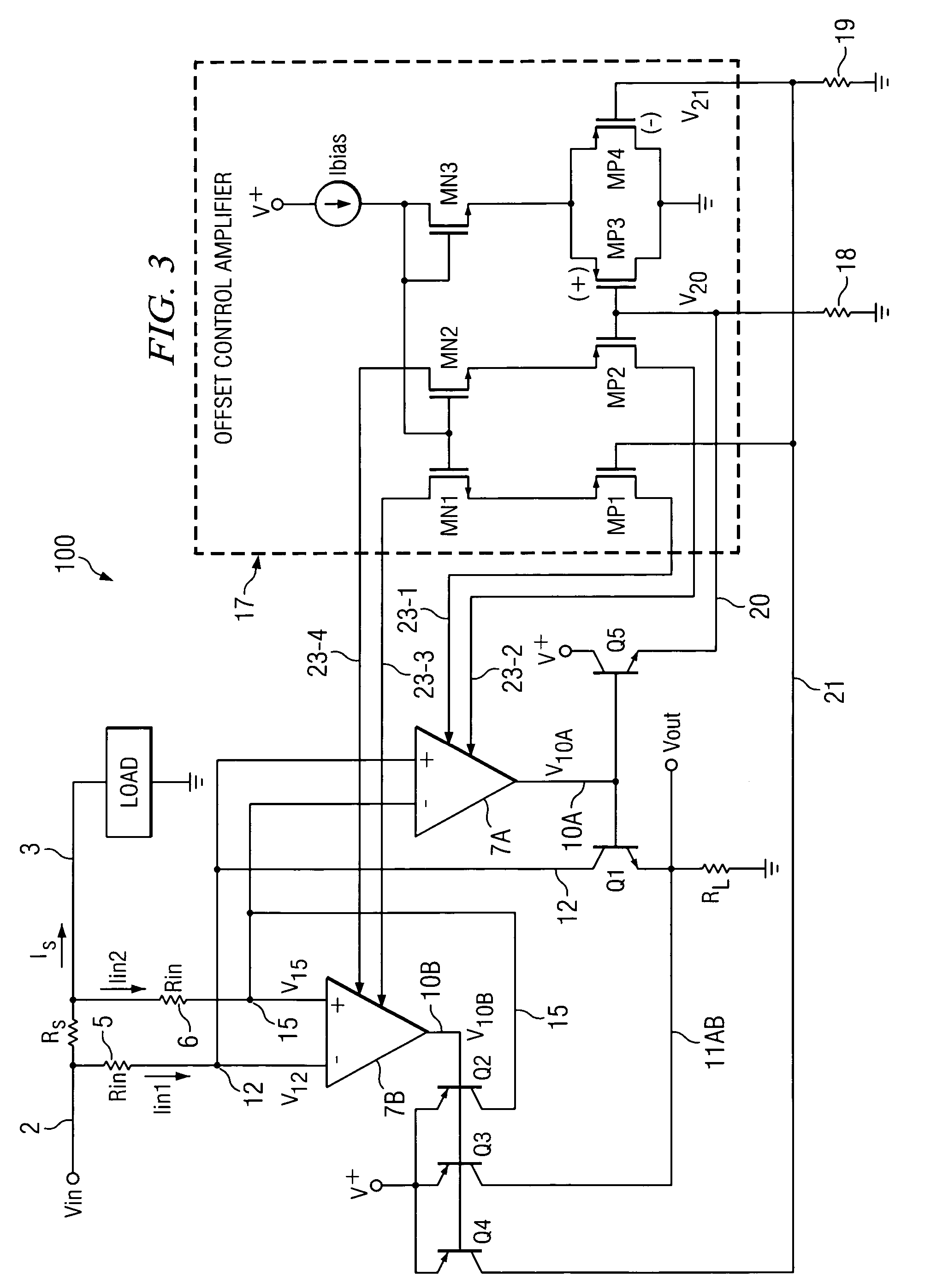
[0025]Referring to FIG. 2, instrumentation amplifier 100 includes the same structure shown in prior art FIG. 1, with operational amplifier 7A having its (−) input connected to conductor 15 and its (+) input connected to conductor 12. As in FIG. 1, conductor 12 is coupled to one terminal of precision input resistor 5, which may, for example, have a resistance Rin equal to 5 kilohms. The other terminal of resistor 5 is coupled by conductor 2 to receive input voltage Vin+ and also is connected to one terminal of sense resistor RS, the other terminal of which is connected by conductor 3 to one terminal of external load 4, the other terminal of which is connected to ground. Sense resistor RS has a very low resistance, typically 10 milliohms, and current IS flows through sense resistor RS into load 4 in response to a positive value of Vin+. The current IS develops a small sense voltage across sense resistor RS. Conductor 3 is connected to one terminal of precision input resistor 6, which ...


PUM


Abstract

An amplifier circuit includes first (7A) and second (7B) operational amplifiers connected in a generally parallel configuration, each with inputs coupled through the same pair of matched input resistors which receive a differential input signal that may have both a positive and negative common mode range. An offset adjustment amplifier (17) receives a differential error signal representative of the difference between offset voltages of the first and second operational amplifiers and generates offset adjustment signals that are applied to input stages of the first and second operational amplifiers to adjust their respective offset voltages so as to equalize them. With the offset voltages equalized, the first and second operational amplifiers operate seamlessly as a common mode component of the differential input signal undergoes a transition from its positive to its negative range, so as to avoid inaccuracies and abrupt changes in an output voltage during the transition, the output voltage being produced in response to outputs of both first and second operational amplifiers.

Description

BACKGROUND OF THE INVENTION[0001]The present invention relates generally to instrumentation amplifiers, and more particularly to circuitry and techniques for providing “seamless” or continuous circuit operation between positive and negative portions of a common mode input range.[0002]The closest prior art is believed to be the assignee's INA 168 positive common mode voltage instrumentation amplifier, a diagram of which is shown in FIG. 1. Referring to FIG. 1, prior art instrumentation amplifier 1 has positive common mode voltage operation between a single supply voltage V+ and ground. Amplifier 1 includes an operational amplifier 7A having a (+) input coupled by a conductor 12 to one terminal of a precision input resistor 5, which may, for example, have a resistance Rin equal to 5 kilohms. The other terminal of resistor 5 is coupled by a conductor 2 to receive an input voltage Vin+ and also is connected to one terminal of a sense resistor Rs, the other terminal of which is connected...

Claims


Application Information

Patent Timeline
Patent Type & Authority Patents(United States)
IPC IPC(8): H03F3/45
CPCH03F3/45192H03F3/45475H03F3/45973H03F2203/45521H03F2200/261
Inventor GAMMIE, DAVID A.ALENIN, SERGEY V.
Owner TEXAS INSTR INC
Why Eureka
Try Eureka