

Heating device
- Summary
- Abstract
- Description
- Claims
- Application Information
AI Technical Summary
Benefits of technology
Problems solved by technology
Method used
Image

Examples
example 1
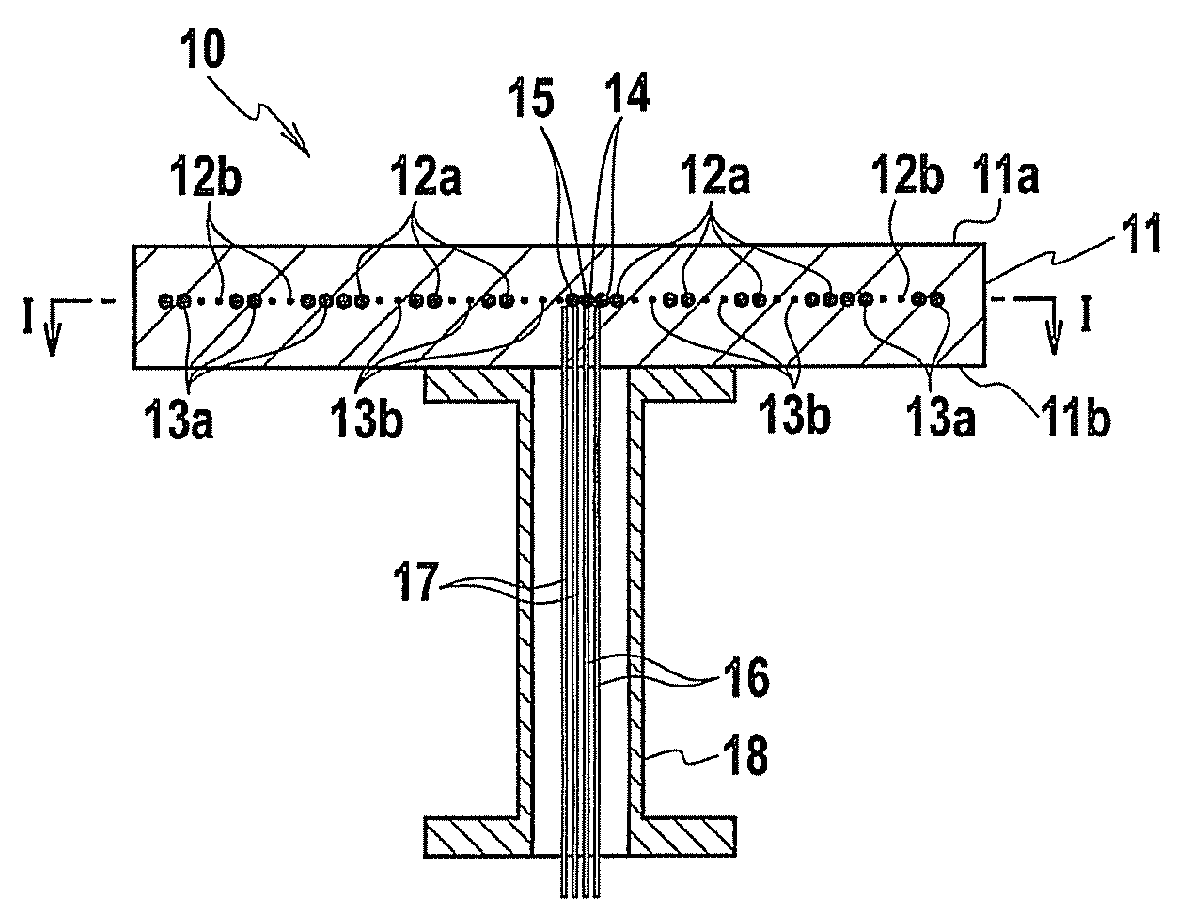
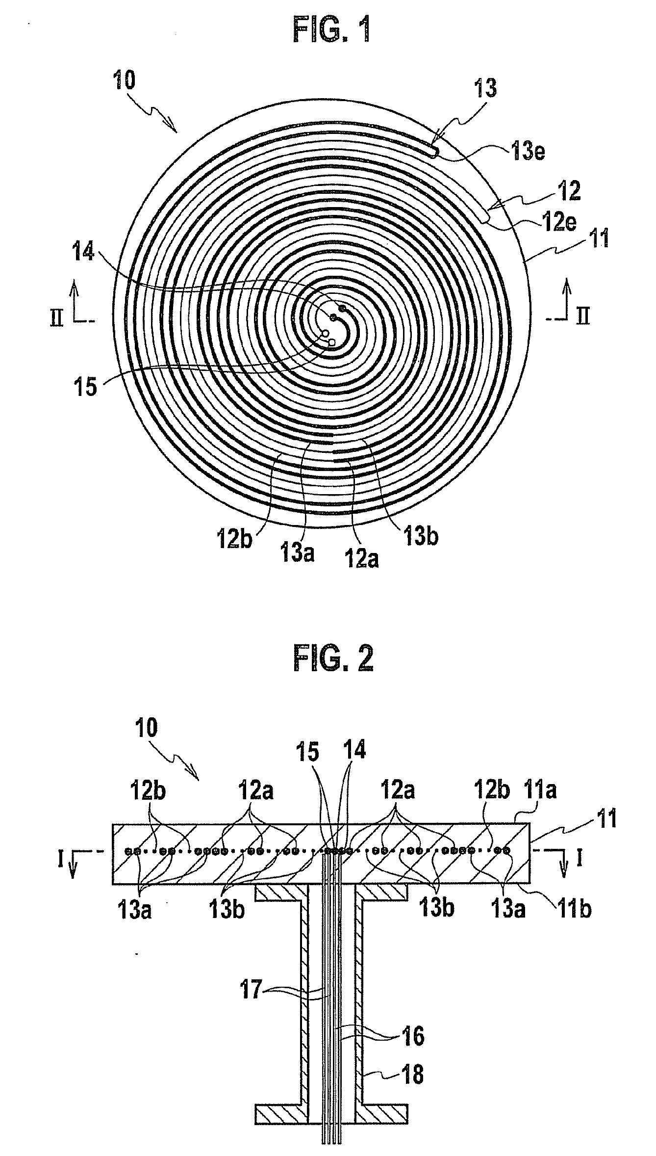
[0052]The heating device 10 having the structure shown in FIG. 1 and FIG. 2 was fabricated. The base 11 was fabricated so as to have a diameter of 320 mm and a thickness of 10 mm. Aluminum nitride was used as the material of the base 11. In the inside of the base 11, the first heating element 12 and the second heating element 13 (made of molybdenum as the material thereof and formed of coil-like heating elements) were individually embedded in the base 11 in the wiring pattern shown in FIG. 1. The first heating element 12 was formed so as to include the high heating density portion 12a on the central portion side of the base 11, and to include, on the peripheral portion side of the base 11, the low heating density portion 12 in which the heating density is lower than that of the high heating density portion 12a. The second heating element 13 was formed so as to include the low heating density portion 13b on the central portion side of the base 11, and to include, on the peripheral po...
example 2
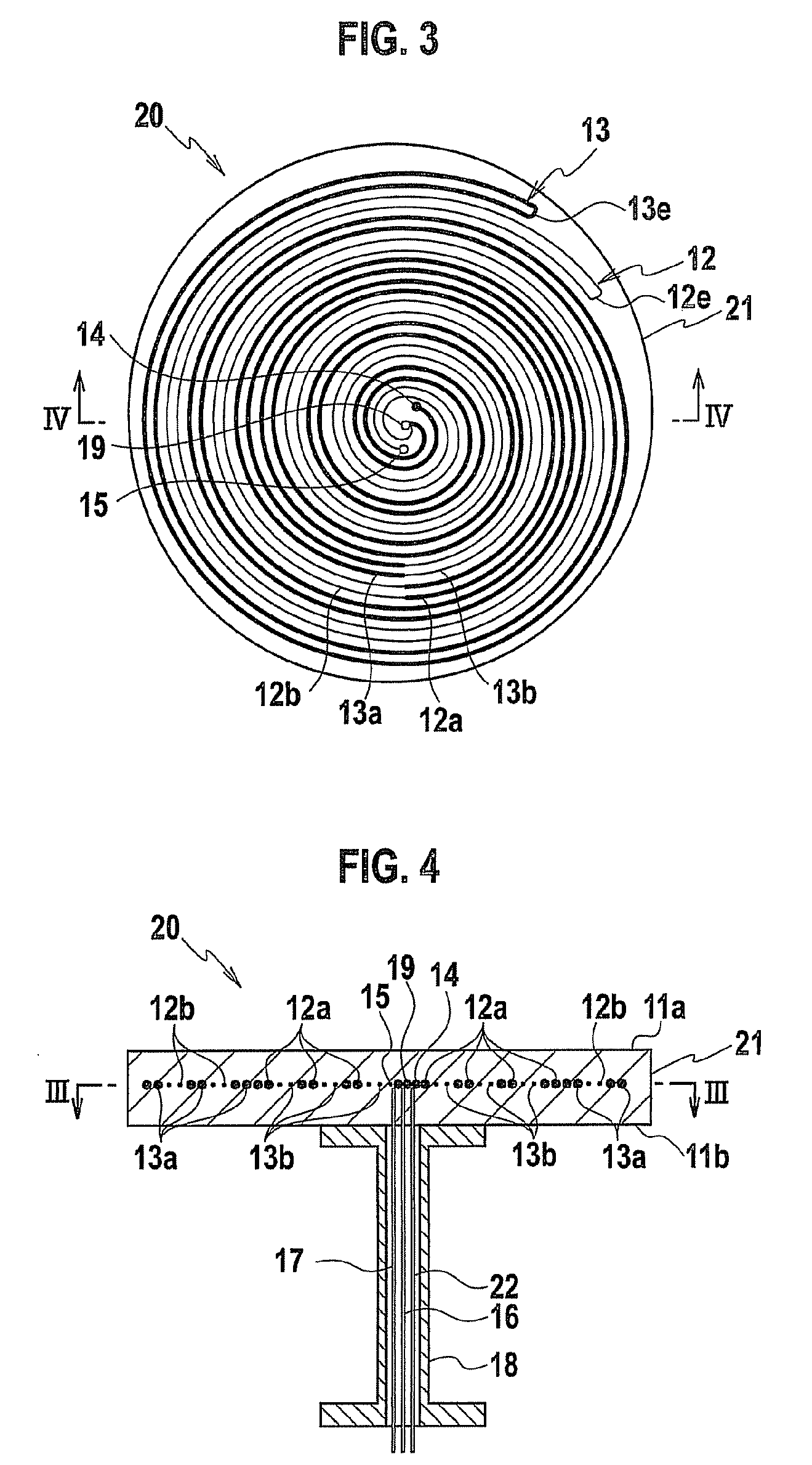
[0055]The heating device 20 having the structure shown in FIG. 3 and FIG. 4 was fabricated. The heating device 20 of this example was different from the heating device 10 of Example 1 in the following points. The heating device 20 includes the common terminal 19 in which one of the two terminals connected to the first heating element 12 and one of the two terminals connected to the second heating element 13 are shared. Moreover, in the heating device 20, the shared power feeding bar 22 is connected to this common terminal. The heating device 20 is similar to the heating device 10 of Example 1 except these points.
[0056]A semiconductor wafer was heated by using the heating device 20 thus fabricated. Then, when the set temperature was 700° C., the temperature distribution (ΔT) on the heating surface 11a of the base 11 became equal to 4° C., and better uniform heating performance than the heating device 10 having the structure shown in FIG. 1 and FIG. 2 was able to be achieved. In gener...
PUM
 Abstract
Description
Claims
Application Information