Active matrix using hybrid integrated circuit and bipolar transistor

Active Publication Date: 2014-12-09
GLOBALFOUNDRIES US INC
View PDF13 Cites 181 Cited by
  • Summary
  • Abstract
  • Description
  • Claims
  • Application Information

AI Technical Summary

Benefits of technology

[0009]A pixel circuit for an active matrix display includes a junction field effect transistor (JFET) enabled by a select signal, and a bipolar junction coupled to the JFET to receive data through the JFET, when enabled, at a base of the bipolar junction, the JFET and the bipolar junction including a crystalline channel material. An organic light emitting diode (OLED) is connected on one side between one of an emitter and a collector of the bipolar junction and, on the other side, between one of supply voltage and ground.
[0010]A method for forming a hybrid integrated circuit device includes doping a base subst

Problems solved by technology

However, the poor mobility and stability of these devices is not sufficient for very high-resolution and low-power displays, such as, e.g., pico-projectors and micro-displays.
The limited performance of these conventional devices (particularly with respect to mobility and therefore drive current and switching speed) is limited by the non-crystalline nature of th

Method used


Image

  • Active matrix using hybrid integrated circuit and bipolar transistor
  • Active matrix using hybrid integrated circuit and bipolar transistor
  • Active matrix using hybrid integrated circuit and bipolar transistor

Examples


Embodiment Construction

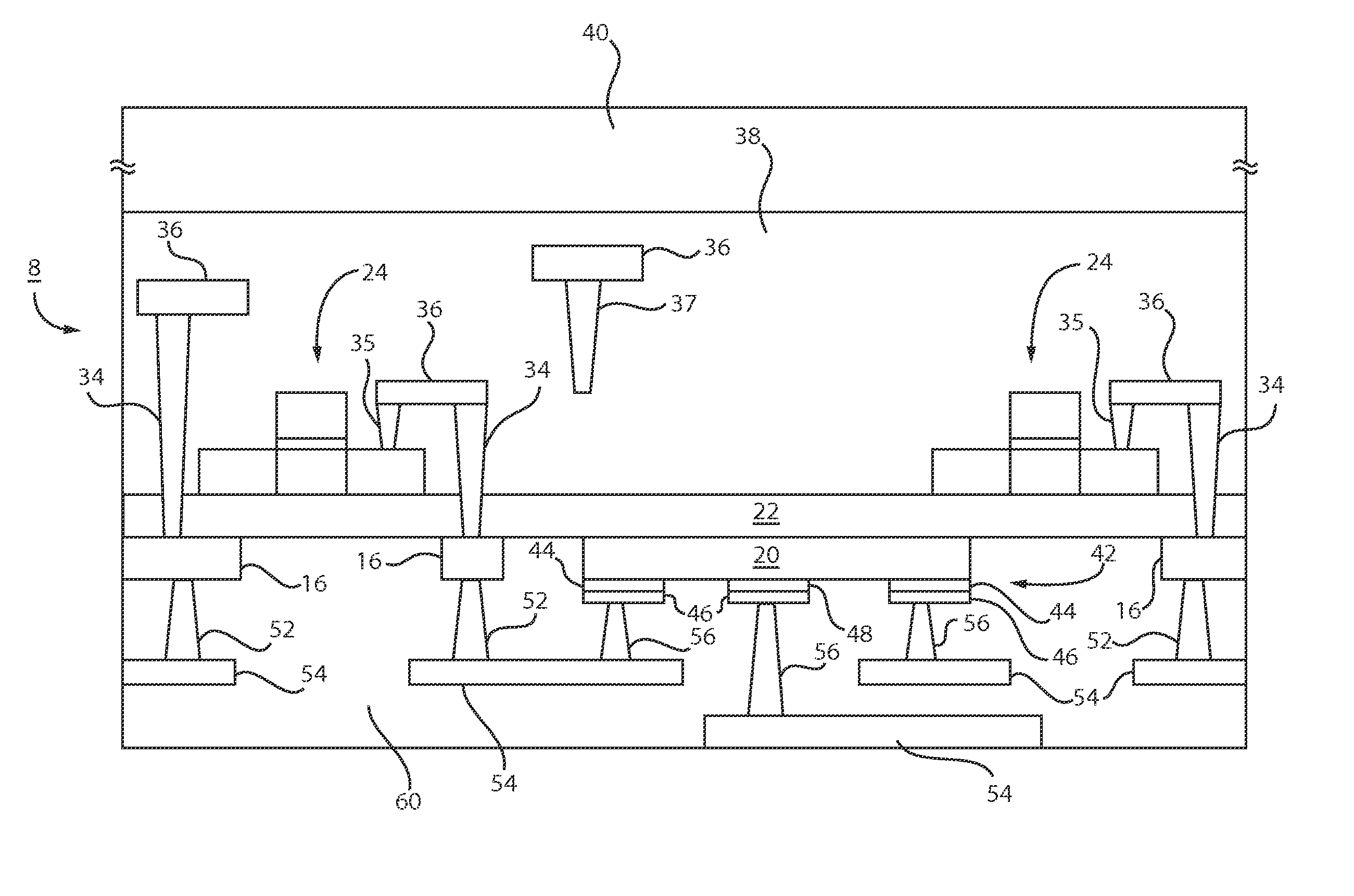
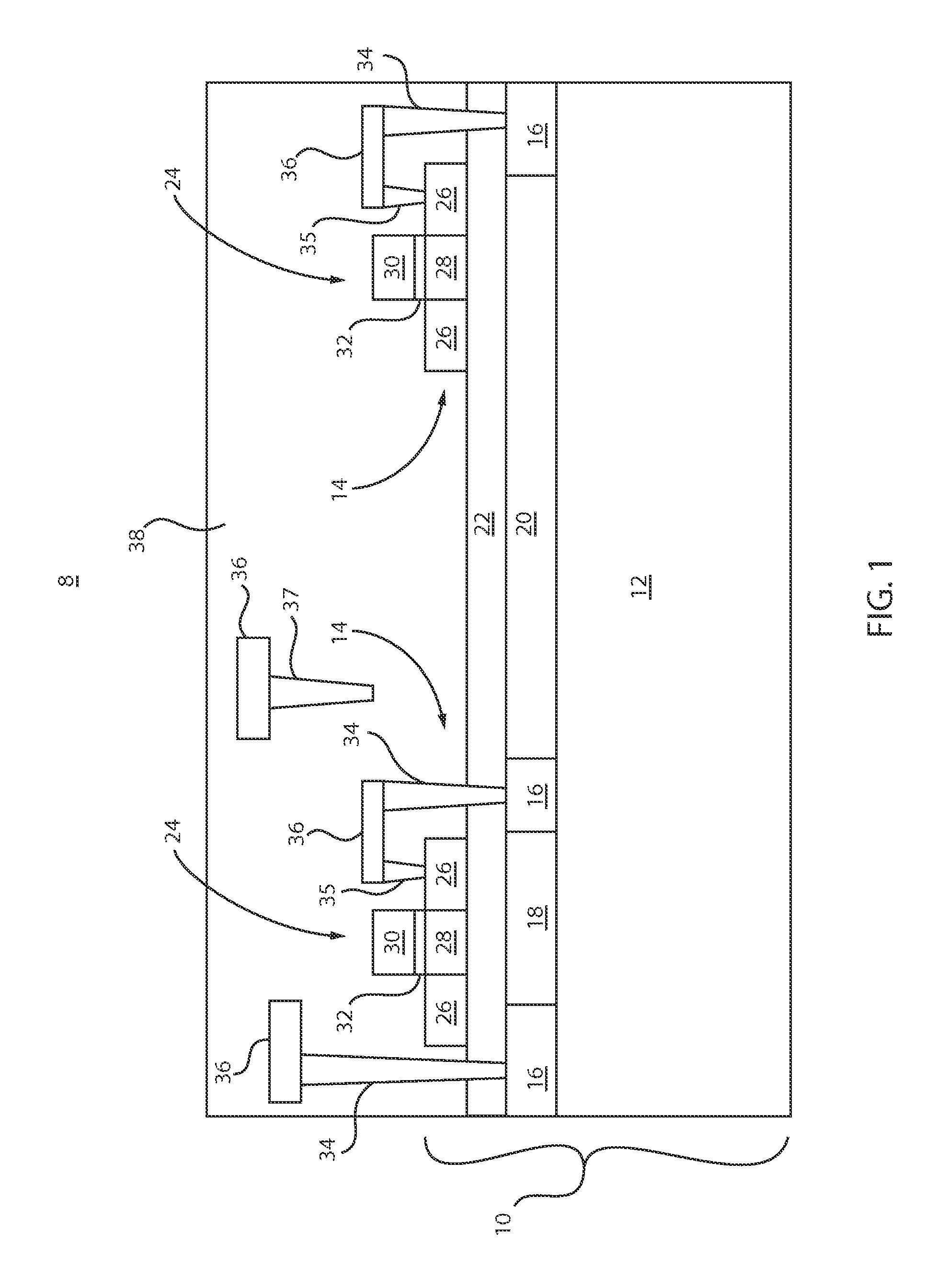
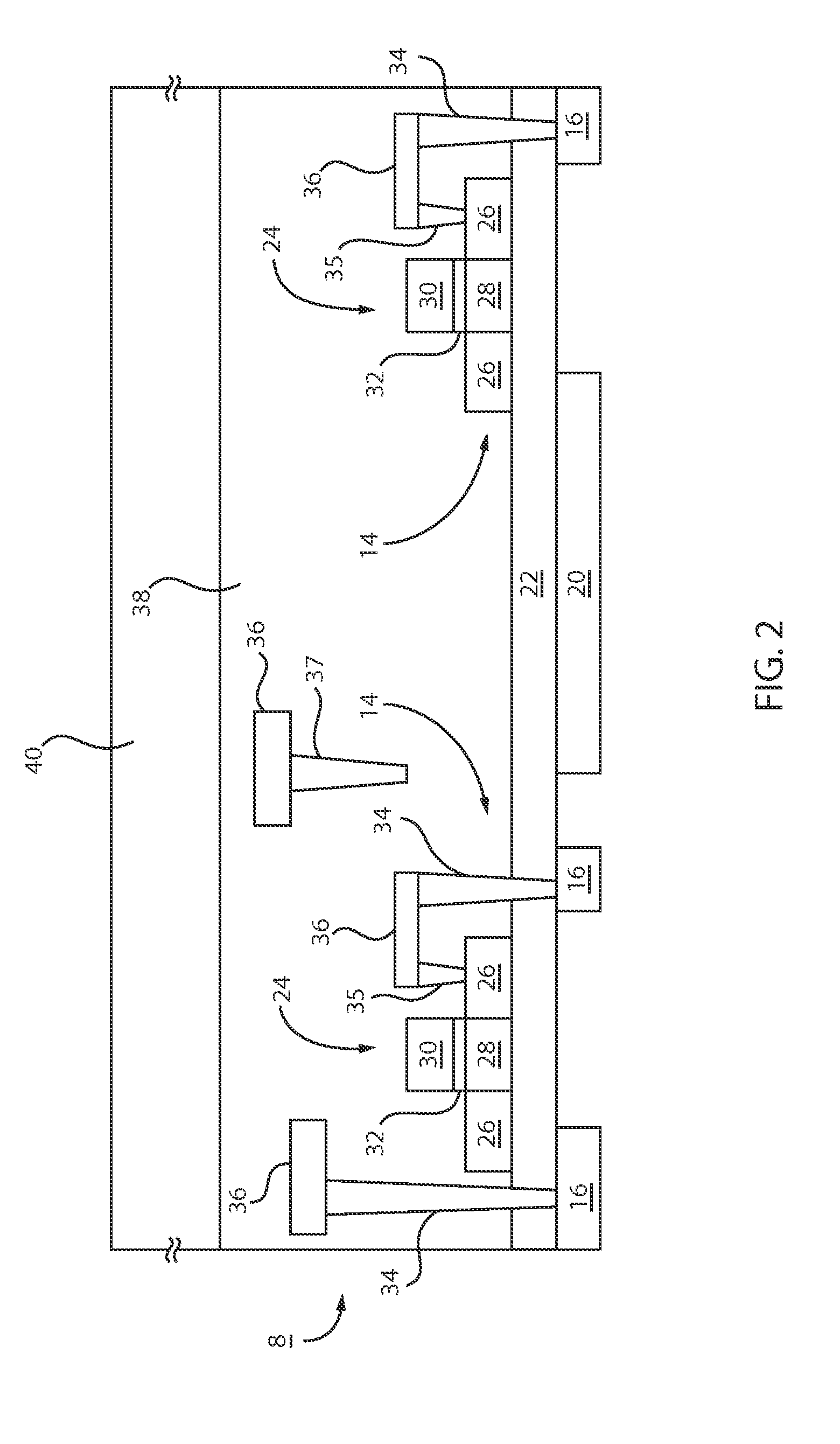
[0030]In accordance with the present principles, devices and methods for fabricating an active matrix display are disclosed. In one embodiment, control / driver circuitry is implemented on a semiconductor on insulator (SOI) substrate using VLSI technology, while a thin film transistor (TFT) backplane is implemented on a thinned handle substrate. The control / driver circuitry may be connected to the back-plane using through-substrate vias or through-silicon vias (TSVs). The TFTs are formed by heterojunction contacts grown at low-temperatures, which do not affect the driver / control circuitry. The performance of the TFTs substantially exceeds that of non-crystalline materials due to the use of the crystalline handle substrate material as the TFT channel. It should be understood that the present principles are not limited to active matrices and the circuitry on the front and the TFTs on the handle substrate may be used for any known application. For example, the TFTs can be used to impleme...


PUM


Abstract

A hybrid integrated circuit device includes a semiconductor-on-insulator substrate having a base substrate, a semiconductor layer and a dielectric layer disposed therebetween, the base substrate being reduced in thickness. First devices are formed in the semiconductor layer, the first devices being connected to first metallizations on a first side of the dielectric layer. Second devices are formed in the base substrate, the second devices being connected to second metallizations formed on a second side of the dielectric layer opposite the first side. A through via connection is configured to connect the first metallizations to the second metallizations through the dielectric layer. Pixel circuits and methods are also disclosed.

Description

RELATED APPLICATION DATA[0001]This application is a Continuation application of co-pending U.S. patent application Ser. No. 13 / 949,498 filed on Jul. 24, 2013, incorporated herein by reference in its entirety.BACKGROUND[0002]1. Technical Field[0003]The present invention relates to integrated circuits, and more particularly to active matrix circuits and fabrication processes having hybrid devices and bipolar transistors integrated therein.[0004]2. Description of the Related Art[0005]In applications such as active-matrix displays, control / driving circuitry is implemented with standard very large scale integration (VLSI) devices and connected to a back-plane (an array of thin film transistors (TFTs) used for driving passive elements such as organic light emitting diodes (OLEDs) and liquid crystal displays (LCDs)) externally. The TFTs are typically comprised of a-Si:H or metal-oxide semiconductors because of their low-cost, large-area compatibility and low deposition temperatures, which ...

Claims


Application Information

Patent Timeline
IPC IPC(8): H01L21/00H01L27/32
CPCH01L27/326H01L27/3276G09G3/32H01L23/5226H01L27/0694H01L27/1207H01L27/3244H01L2924/0002G09G3/3225G09G2300/0842H10K59/12H01L2924/00H10K59/131H10K59/121H10K59/1216H10K2102/3026H10K2102/3035H01L29/04H01L29/1004H01L29/16H01L29/73H01L29/808
Inventor HEKMATSHOARTABARI, BAHMANNING, TAK H.SHAHIDI, GHAVAM G.SHAHRJERDI, DAVOOD
Owner GLOBALFOUNDRIES US INC
Why Eureka
Try Eureka