Design structure for electrically tunable resistor

a design structure and resistor technology, applied in the field of integrated circuit (ic) chips, can solve the problems of cost, limited deposition materials, and control of resistan

Active Publication Date: 2008-10-02
TAIWAN SEMICON MFG CO LTD
View PDF32 Cites 0 Cited by
  • Summary
  • Abstract
  • Description
  • Claims
  • Application Information

AI Technical Summary

Benefits of technology

[0011]A third aspect of the disclosure provides a method of forming a resistor, the method comprising: providing a first plurality of layers of different materials; first passing a current pulse through the first plurality of layers to affect a conductivity structure of the first plurality of layers in order to obtain a first predetermined resistance value for the resistor; measuring a resistance of the first plurality of layers; determining a calibration for tuning the resistance based on the measuring; providing at least one second plurality of layers of different materials substantially identical to the first plurality of layers; and second passing a current pulse through each of the at least one second plurality of layers to affect a conductivity structure of each second plurality of layers in order to obtain a second predetermined resistance value different from the first predetermined resistance value.

Problems solved by technology

A number of challenges exist relative to controlling the resistance.
Third, new variations in the resistance values derived by changing the resistor geometry require new masks to make specialty IC chips.
Finally, changes in the resistance from a variation in material resistivity rho require a change of the deposition material, which is costly and limited by available deposition materials.

Method used


Image

  • Design structure for electrically tunable resistor
  • Design structure for electrically tunable resistor
  • Design structure for electrically tunable resistor

Examples


Embodiment Construction

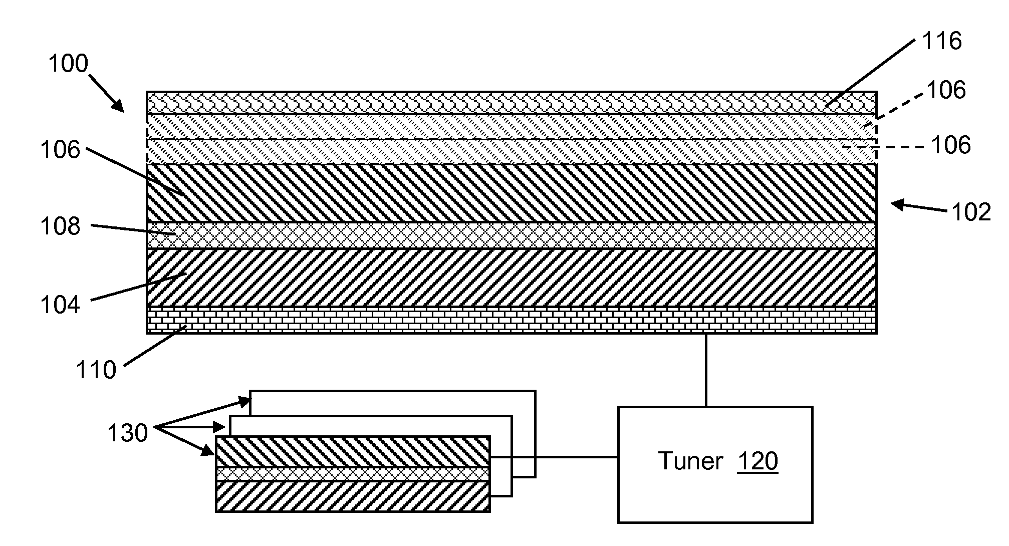
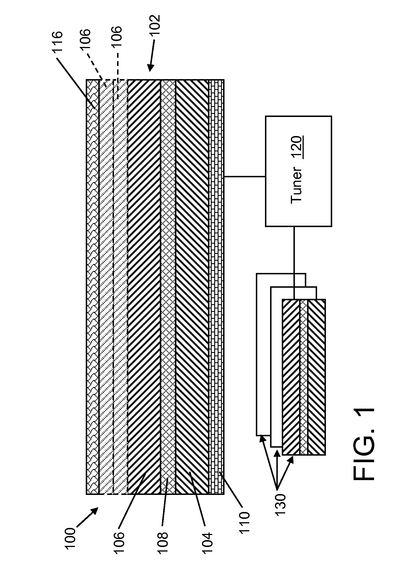
[0019]Referring to FIG. 1, one embodiment includes a method of forming a resistor 100. First, a plurality of layers 102 of different materials is provided. As shown, plurality of layers 102 includes a first resistive layer 104 and at least one second resistive layer 106. Any number of second resistive layer(s) 106 may be employed. Resistive layers 104, 106 may include any now known or later developed resistive material. However, in one embodiment, resistive layers 104, 106 each include a conductive material such as a metal. Where metals are used, resistive layers 104, 106 of, for example, iron (Fe) and cobalt (Co), respectively, may be employed. First resistive layer 104 may include a first metal material and at least one second resistive layer 106 may include at least one other different metal material. Other materials may also be employed including but not limited to chromium (Cr), copper (Cu), silver (Au), gold (Ag), aluminum (Al), ruthenium (Ru), platinum (PI), tantalum (Ta), mo...


PUM


Abstract

A design structure for an electrically tunable resistor. In one embodiment, the design structure is embodied in a machine readable medium for designing, manufacturing, or testing an integrated circuit, and includes a resistor including: a first resistive layer; at least one second resistive layer; and an intermediate interdiffused layer of the first resistive layer and the at least one second resistive layer.

Description

CROSS-REFERENCE TO RELATED APPLICATIONS[0001]This patent application is a continuation-in-part of U.S. patent application Ser. No. 11 / 691,755, filed Mar. 27, 2007.BACKGROUND OF THE DISCLOSURE[0002]1. Technical Field[0003]The disclosure relates generally to integrated circuit (IC) chips, and more particularly, to design structure for an electrically tunable resistor.[0004]2. Background Art[0005]Thin film resistors are used in the integrated circuit (IC) chip industry. The resistance R of a rectangular sheet of material of width W, height H and thickness d is determined by the film resistivity (rho) by: R=rho*W / (H*d). Any of the above mentioned parameters can be varied to vary the resistance R.[0006]A number of challenges exist relative to controlling the resistance. First, if different resistance values in a circuit are desired, the geometric parameters width W, height H or thickness d, and / or the material resistivity rho, must be varied. Second, tolerance variations in material resi...

Claims


Application Information

Patent Timeline
Patent Type & Authority Applications(United States)
IPC IPC(8): H01L21/66
CPCH01C10/14H01L22/34H01L28/20H01L28/24H01L2924/0002H01L2924/00
Inventor IBEN, ICKO E. T.STRONG, ALVIN W.
Owner TAIWAN SEMICON MFG CO LTD
Why Eureka
Try Eureka