Semiconductor device and method of fabricating the same

a technology of semiconductors and devices, applied in the field of integrated circuits, can solve the problems of limited application area of transistors and device operation problems, and achieve the effect of enhancing the efficiency of devices in the core circui

Inactive Publication Date: 2008-10-02
UNITED MICROELECTRONICS CORP
View PDF4 Cites 6 Cited by
  • Summary
  • Abstract
  • Description
  • Claims
  • Application Information

AI Technical Summary

Benefits of technology

[0008]The present invention is to provide a semiconductor device and a fabrication method thereof, wherein the efficiency of the dev

Problems solved by technology

However, limited by the mobility rate of electrons and holes in the silicon channel, the area of application of the transistor is limited.
The electrical properti

Method used


Image

  • Semiconductor device and method of fabricating the same
  • Semiconductor device and method of fabricating the same
  • Semiconductor device and method of fabricating the same

Examples


Embodiment Construction

[0038]According to a fabrication method of a semiconductor device of the present invention, a strain process is performed on the devices of the core circuit region, but not on the devices of the non-core circuit region to enhance the efficiency of the devices of the core circuit region, while maintain the operational characteristics of the devices of the non-core circuit region. The strain process alters the material of the source / drain region of the core circuit region to a semiconductor compound, and / or forms a stress layer on the devices of the core circuit region.

[0039]The present invention is illustrated by the following two embodiments. However, it is to be understood that these embodiments are presented by way of example and not by way of limitation.

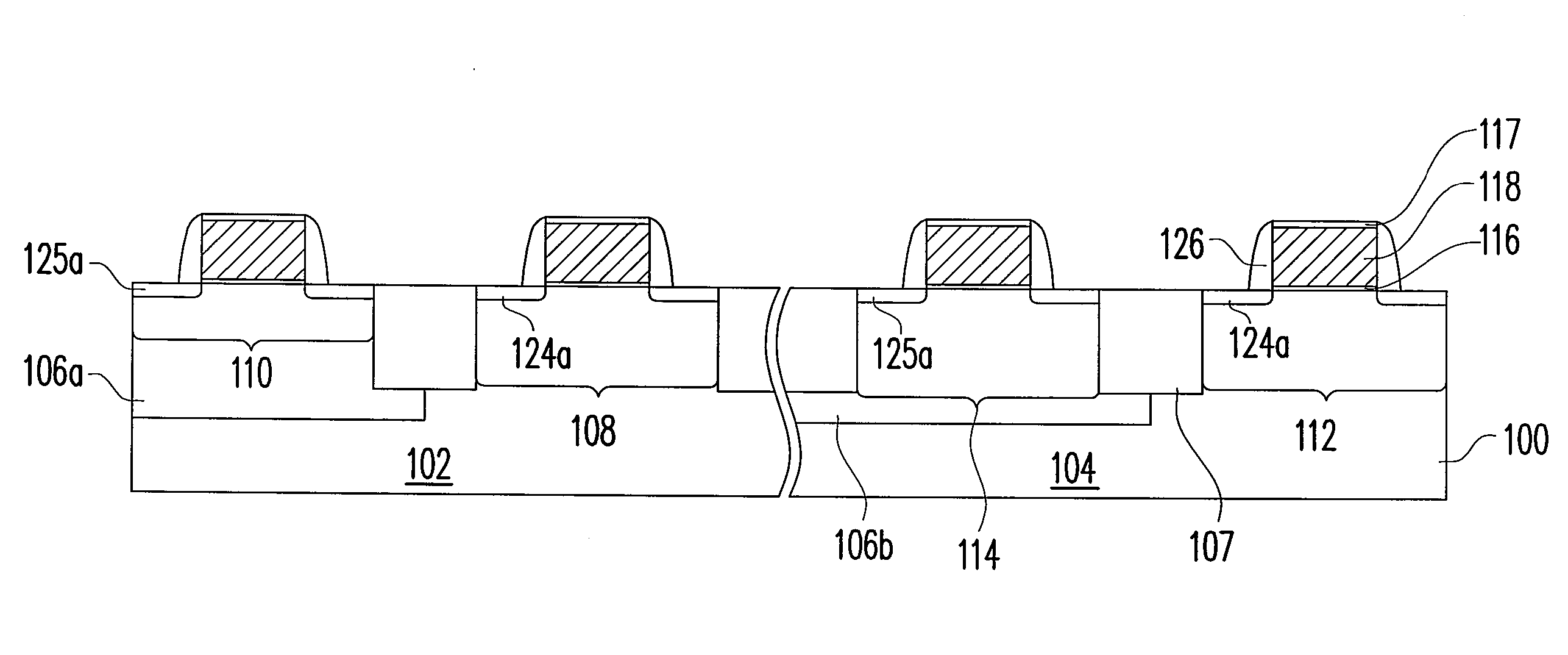
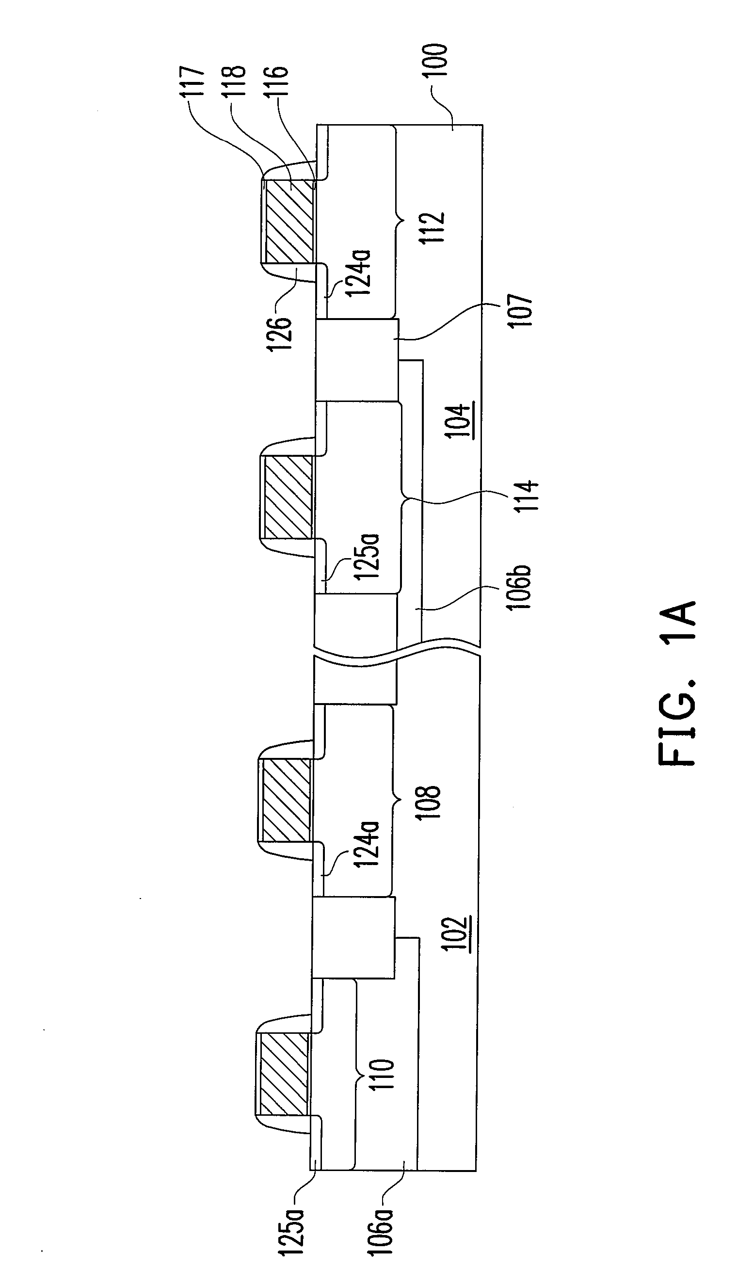
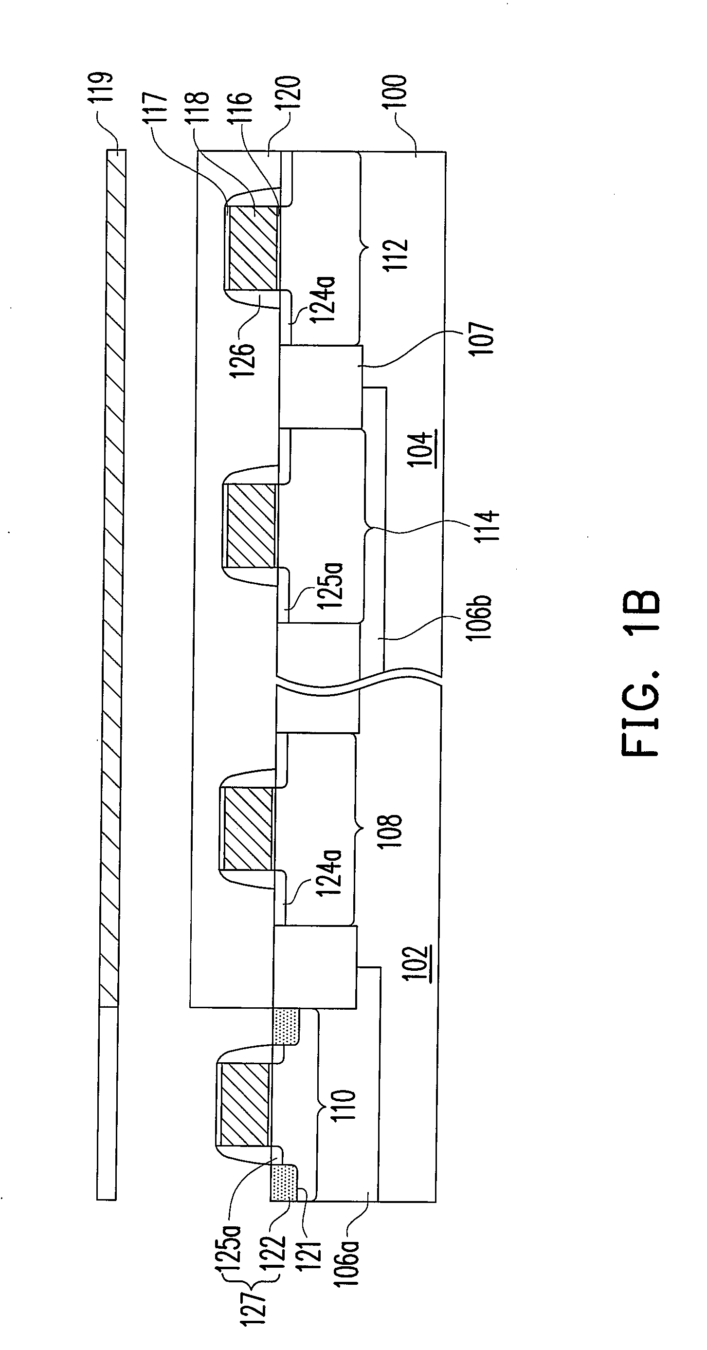
[0040]FIGS. 1A to 1E are cross-sectional views showing selected process steps for fabricating a semiconductor device according an embodiment of the invention.

[0041]Referring to FIG. 1A, a substrate 100 is provided, wherein a mater...


PUM


Abstract

A method of fabricating a semiconductor device is provided. Devices are formed on a core region and a non-core region in a substrate. A strain process is performed to the device on the core region but is not performed to the device on the non-core region.

Description

BACKGROUND OF THE INVENTION[0001]1. Field of Invention[0002]The present invention relates to an integrated circuit and a method for fabricating the same. More particularly, the present invention relates a semiconductor device and a method for fabricating the same.[0003]2. Description of Related Art[0004]Along with the development of the technology in electronic equipments for communication, etc., the operating speed of a transistor increases rapidly. However, limited by the mobility rate of electrons and holes in the silicon channel, the area of application of the transistor is limited.[0005]Relying on the mechanical stress in the channel to control the mobility rate of electrons and holes in the channel is one approach to enhance the operational speed of a transistor.[0006]Conventionally, the silicon germanium (SiGe) type of material has been proposed for forming the source / drain regions of the transistor, wherein portions of the substrate pre-determined for forming the source / drai...

Claims


Application Information

Patent Timeline
IPC IPC(8): H01L29/94H01L21/00H01L21/336
CPCH01L21/823412H01L21/823807H01L29/665H01L29/6659H01L29/7833H01L29/7843
Inventor YANG, CHIN-SHENG
Owner UNITED MICROELECTRONICS CORP
Why Eureka
Try Eureka