Single electron transistor and method of manufacturing the same

a single electron transistor and manufacturing method technology, applied in the field of single electron transistors, can solve the problems of difficult uniform formation of quantum dots, unexpected problems may arise and various technical difficulties in attempting to redu

Active Publication Date: 2008-10-09
SAMSUNG ELECTRONICS CO LTD
View PDF9 Cites 63 Cited by
  • Summary
  • Abstract
  • Description
  • Claims
  • Application Information

AI Technical Summary

Benefits of technology

[0008]Embodiments are therefore directed to a single electron transistor and a method of manufacturing the same, wh

Problems solved by technology

However, various technical difficulties may arise in attempting such a reduction.
Further, even when the sizes are reduced, unexpected problems may be undesirably generated.
However, quantum dots are difficult to form uniformly with conventional techniques, and thus the SET has not been made easily m

Method used


Image

  • Single electron transistor and method of manufacturing the same
  • Single electron transistor and method of manufacturing the same
  • Single electron transistor and method of manufacturing the same

Examples


Embodiment Construction

[0039]Korean Patent Application No. 2006-97507, filed on Oct. 4, 2006, in the Korean Intellectual Property Office, and entitled: “Single Electron Transistor and Method of Manufacturing the Same,” is incorporated by reference herein in its entirety.

[0040]Example embodiments will now be described more fully hereinafter with reference to the accompanying drawings; however, they may be embodied in different forms and should not be construed as limited to the embodiments set forth herein. Rather, these embodiments are provided so that this disclosure will be thorough and complete, and will fully convey the scope of the invention to those skilled in the art. In the figures, the dimensions of layers and regions may be exaggerated for clarity of illustration. Like reference numerals refer to like elements throughout.

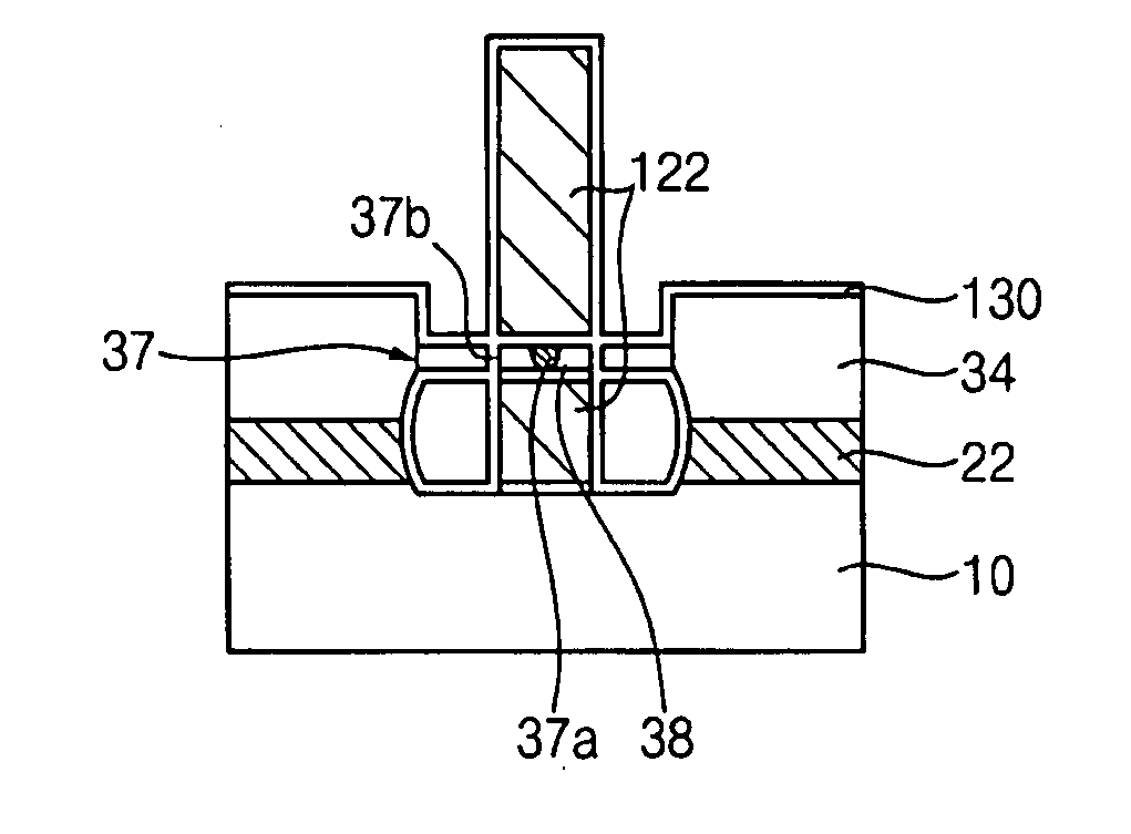
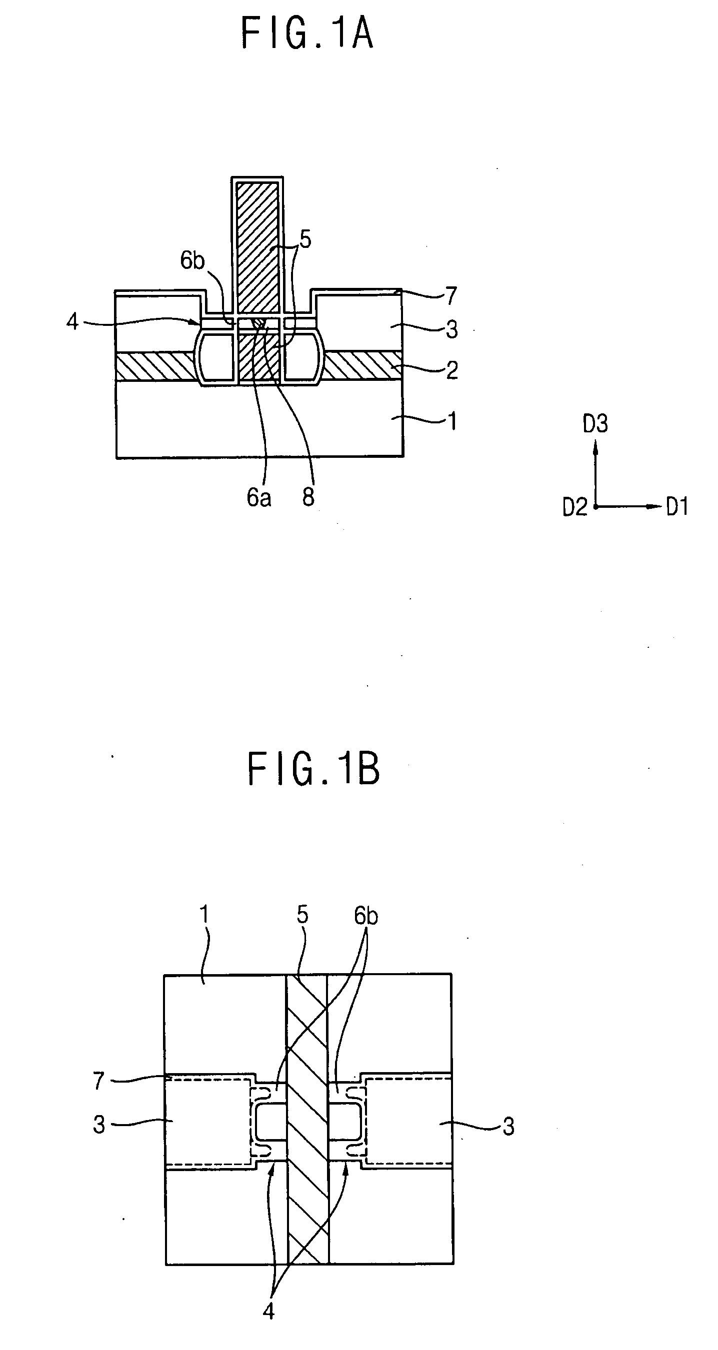
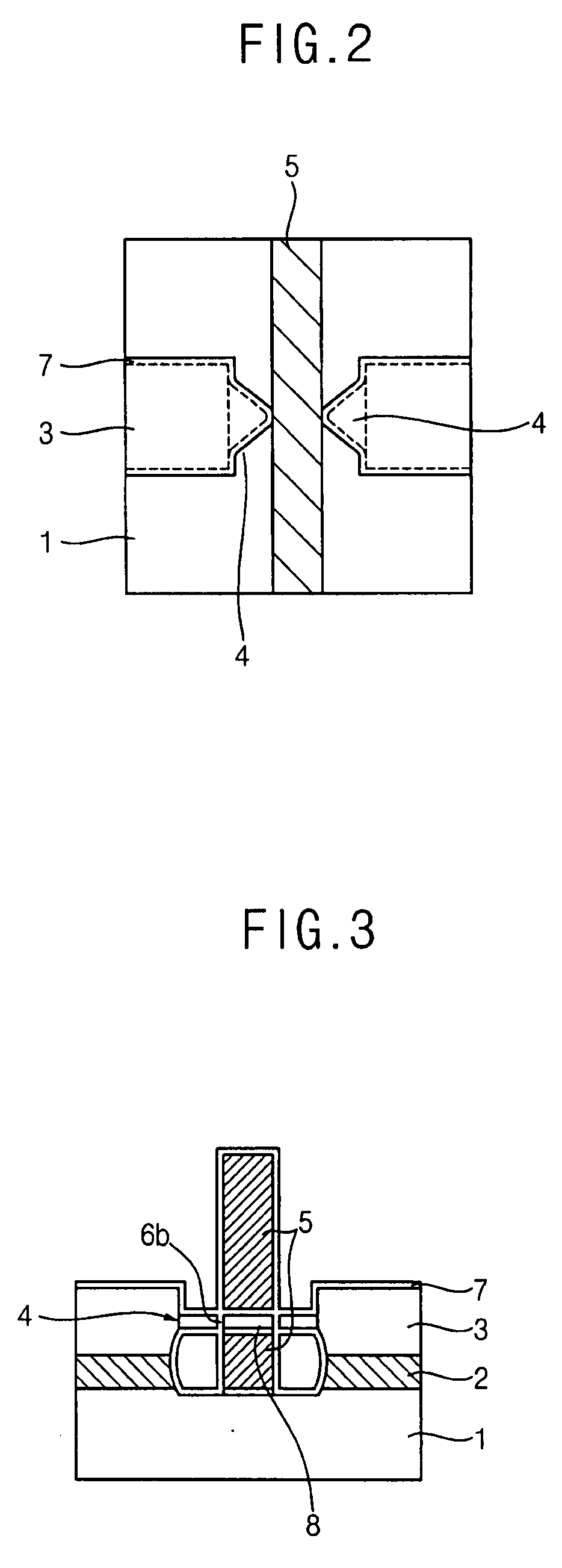
[0041]FIG. 1A illustrates a cross-sectional view of a single electron transistor in accordance with an example embodiment, and FIG. 1B illustrates a top view of the single elect...


PUM


Abstract

A single electron transistor includes source/drain layers disposed apart on a substrate, at least one nanowire channel connecting the source/drain layers, a plurality of oxide channel areas in the nanowire channel, the oxide channel areas insulating at least one portion of the nanowire channel, a quantum dot in the portion of the nanowire channel insulated by the plurality of oxide channel areas, and a gate electrode surrounding the quantum dot.

Description

BACKGROUND OF THE INVENTION[0001]1. Field of the Invention[0002]Example embodiments relate to a semiconductor device and a method of manufacturing the same and, more particularly, to a single electron transistor and a method of manufacturing the same.[0003]2. Description of the Related Art[0004]In order to increase a degree of integration of a semiconductor device, the size of unit cells should be reduced. However, various technical difficulties may arise in attempting such a reduction. Further, even when the sizes are reduced, unexpected problems may be undesirably generated. For example, electrons in a channel region may be decreased in number to several tens of electrons, and a ratio of the number of electrons corresponding to statistical errors to the number of total electrons operating in the unit cells may be increased, thereby affecting a reliability of the operations of the unit cells. Thus, there is a demand for unit cells having a structure suitable for a high degree of in...

Claims


Application Information

Patent Timeline
IPC IPC(8): H01L29/12H01L21/336
CPCB82Y10/00H01L29/66439H01L29/7613Y10S438/962Y10S977/937Y10S977/938H01L29/0669
Inventor SUK, SUNG-DAEYEO, KYOUNG-HWANLI, MINGYEOH, YUN-YOUNG
Owner SAMSUNG ELECTRONICS CO LTD
Why Eureka
Try Eureka