
PCM pad design for peeling prevention

Inactive Publication Date: 2008-10-09
TAIWAN SEMICON MFG CO LTD
View PDF6 Cites 4 Cited by
  • Summary
  • Abstract
  • Description
  • Claims
  • Application Information

AI Technical Summary

Benefits of technology

[0009]The present invention has the advantageous features of reduced peeling of PCM residues, and reduced possibility of shortening.

Problems solved by technology

Along with these advancements, the challenges of maintaining yield and throughput have also increased.
However, circuit failure results from the sawing process.
Such a failure is random and hard to predict.
Although changes in design may possibly solve or reduce the problem, such design changes are limited by several factors.
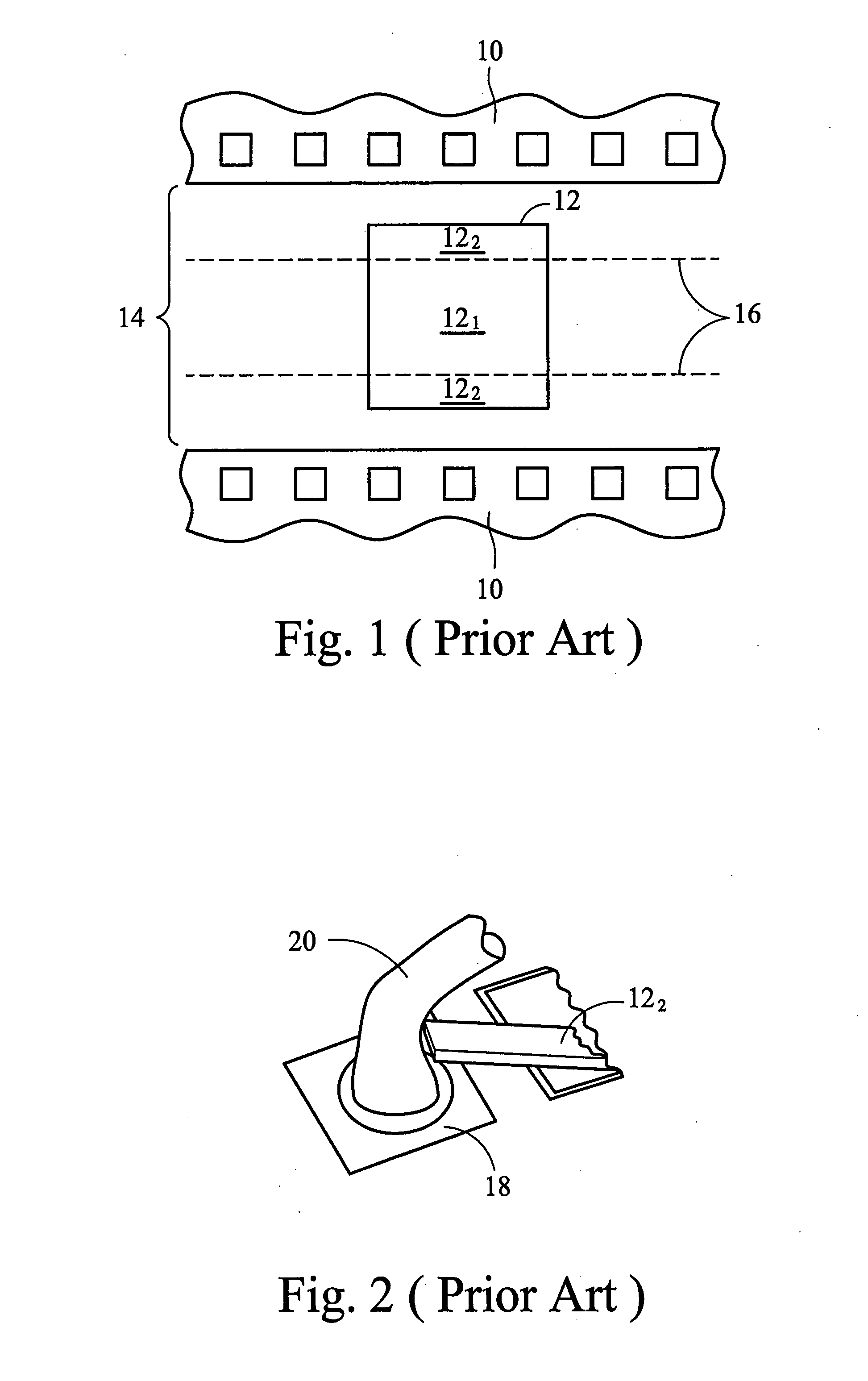
However, the size of test pad 12 is relative to the size of the probe needles, and cannot be reduced as wished as an easy solution for this problem.
However, this solution causes waste of wafer area.
However, wider saws cause the decrease in the distance between the saw and seal rings (not shown) in semiconductor chips, and hence the likelihood of damage to the seal ring increases, wherein damage may be caused by the vibration generated in the sawing process.

Method used


Image

  • PCM pad design for peeling prevention
  • PCM pad design for peeling prevention
  • PCM pad design for peeling prevention

Examples


Embodiment Construction

[0018]The making and using of the presently preferred embodiments are discussed in detail below. It should be appreciated, however, that the present invention provides many applicable inventive concepts that can be embodied in a wide variety of specific contexts. The specific embodiments discussed are merely illustrative of specific ways to make and use the invention, and do not limit the scope of the invention.

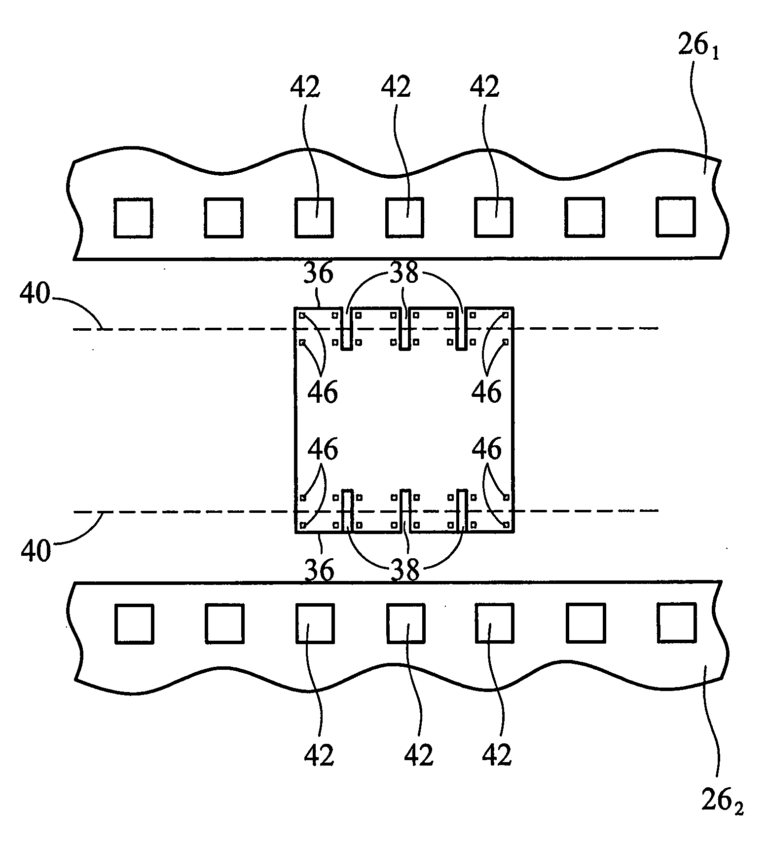
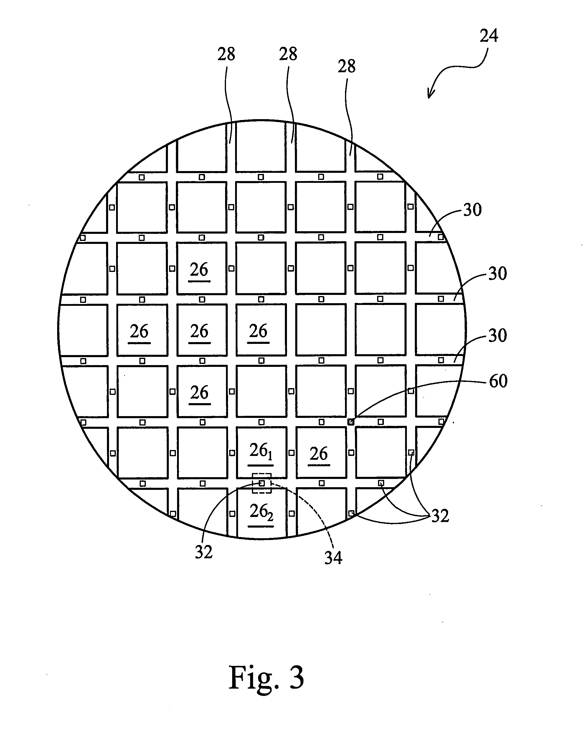
[0019]A novel test pad structure and methods of forming the same are provided. Throughout the various views and illustrative embodiments of the present invention, like reference numbers are used to designate like elements. Referring to FIG. 3, a top view of semiconductor wafer 24 is shown. Semiconductor wafer 24 includes chips (also commonly referred to as dies) 26 separated from each other by first scribe lines 28 and second scribe lines 30. The first scribe lines 28 extend along a first direction and the second scribe lines 30 extend along a second direction perpendicular t...


PUM


Abstract

A semiconductor structure is provided. The semiconductor structure includes a semiconductor chip and a scribe line adjoining the semiconductor chip. A conductive feature is formed in the scribe line and exposed on the surface of the scribe lines, wherein the conductive feature has an edge facing the semiconductor chip. A kerf path is in the scribe line. A first cut is formed in the conductive feature, wherein the first cut extends from the first edge to the kerf path.

Description

TECHNICAL FIELD[0001]This invention relates to the manufacture of semiconductor chips, and more particularly to the design of process control monitor pads.BACKGROUND[0002]Integrated circuit (IC) manufacturers are employing increasingly smaller dimensions and corresponding technologies to make smaller, high-speed semiconductor devices. Along with these advancements, the challenges of maintaining yield and throughput have also increased.[0003]A semiconductor wafer typically includes dies (or chips) separated from each other by scribe lines. Individual chips within the wafer contain circuitry, and the dies are separated by sawing and then are individually packaged. Alternately, the individual chips may be packaged in multi-chip modules. In a semiconductor fabrication process, semiconductor devices on wafers (e.g., an integrated circuit) must be continuously tested at every step of the formation so as to maintain and assure device quality. Usually, a testing circuit is simultaneously fa...

Claims


Application Information

Patent Timeline
IPC IPC(8): H01L23/544H01L21/66
CPCH01L22/34H01L2924/0002H01L2924/00
Inventor TSAI, HAO-YIHSU, SHIH-HSUNCHEN, HSIEN-WEILIU, BENSONTSAI, CHIA-LUNWU, ANBIARSHY N.F.
Owner TAIWAN SEMICON MFG CO LTD
Learn More