Standard cell and semiconductor device including the same
- Summary
- Abstract
- Description
- Claims
- Application Information
AI Technical Summary
Benefits of technology
Problems solved by technology
Method used
Image

Examples
first embodiment
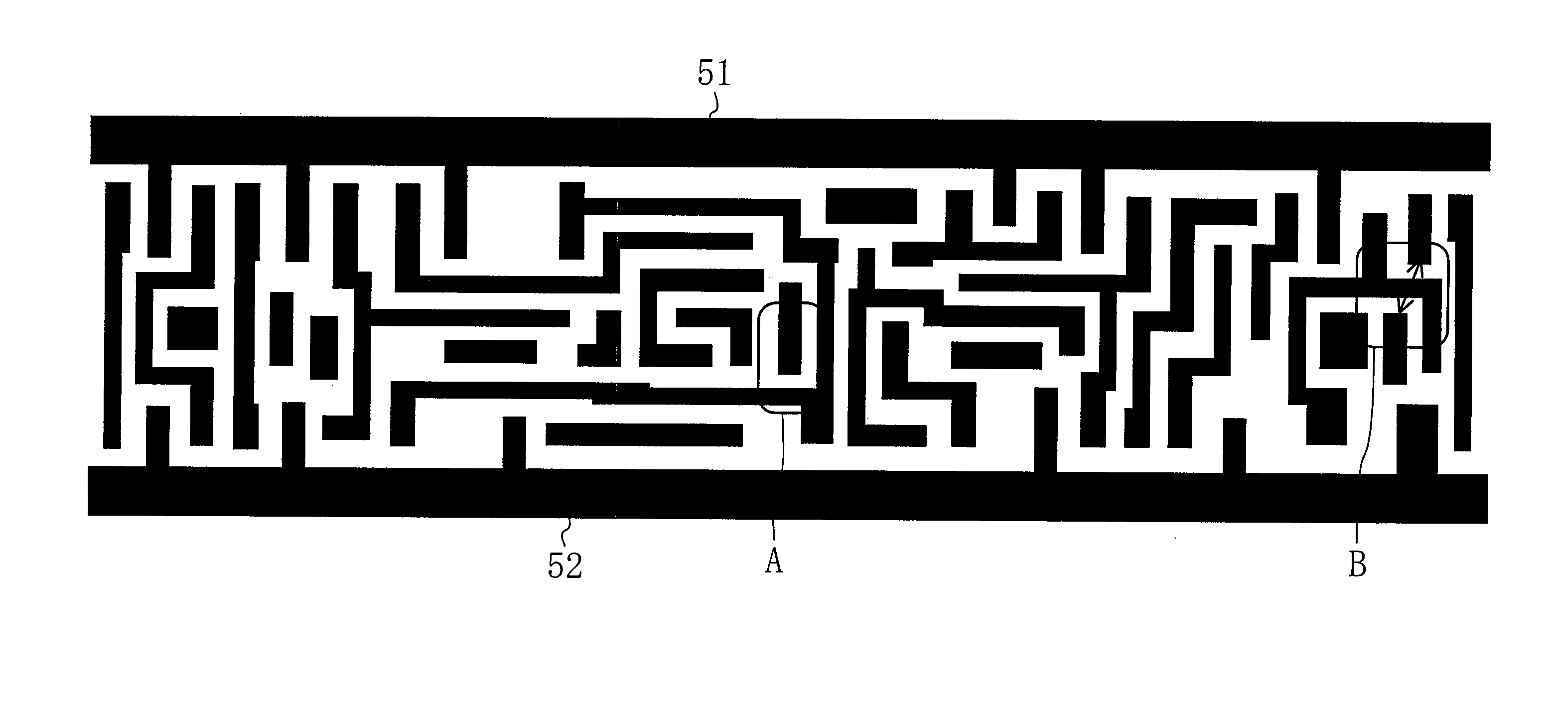
[0035]FIG. 1 is an example of a wiring pattern of a standard cell included in a semiconductor device according to an embodiment of the present invention. FIG. 1 illustrates a wiring pattern in a certain wiring layer. At the upper and lower ends, power lines 51 and 52 are laid out horizontally.
[0036]Each embodiment of the present invention is supposed to employ 45 nm or finer processing. In 45 nm or finer processing, wiring pitch P as shown in FIG. 2, i.e. the center-to-center distance between the wires, is equal to or less than 170 nm. That is, the present invention is based on the premise that the wiring pitch is equal to or less than 170 nm.
[0037]In the present invention, a “signal wire” is defined as a wire other than the wires connected to the power lines. In each drawing, the first direction is defined as a lateral direction, and the second direction substantially perpendicular to the first direction is defined as a vertical direction.
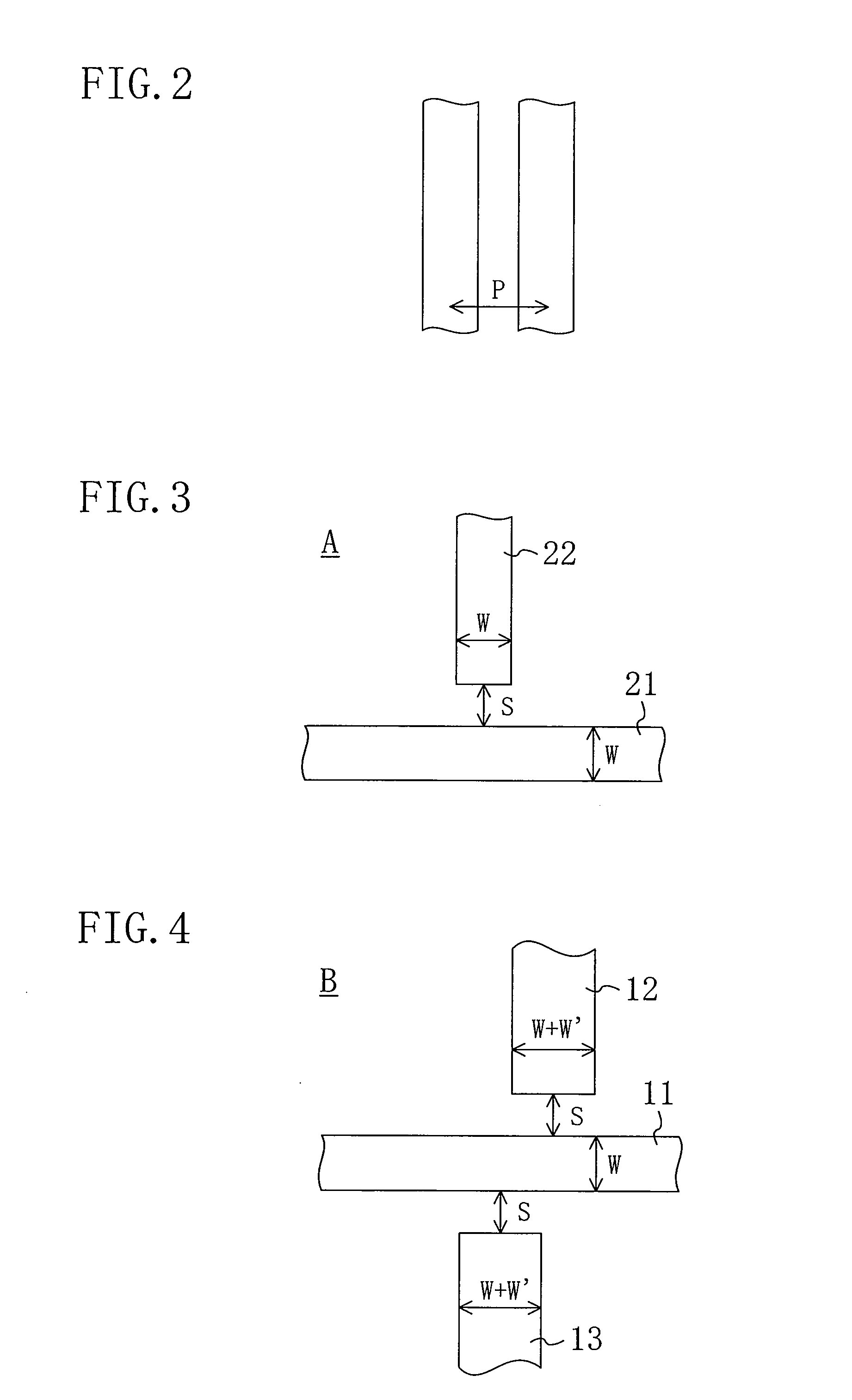
[0038]FIG. 3 is a magnified view of the wir...
second embodiment
[0043]FIG. 6 is a diagram illustrating an improved example, according to this embodiment, of the wiring pattern B in FIG. 1. In FIG. 6, a space between the signal wire 11 and an end of the signal wire 12 is enlarged to S+S′. A space between the signal wire 11 and an end of the signal wire 13 is also enlarged to S+S′. Compared to the wiring pattern A shown in FIG. 3, the space between the signal wire 11 and the end of the signal wire 12 and the space between the signal wire 11 and the end of the signal wire 13 are larger than the space S between the signal wire 21 (fourth signal wire) and the end of the signal wire 22 (fifth signal wire).
[0044]By enlarging the spaces between the interposed signal wire 11 and the ends of the two signal wires 12 and 13 facing each other across the signal wire 11, light interference to the signal wire 11 during exposure is inhibited to prevent attenuation of the signal wire 11.
[0045]Although in the example of FIG. 6, both the signal wires 12 and 13, wit...
third embodiment
[0047]Any signal wire adjacent to a cell border of a standard cell also has a risk of developing attenuation of the wire or causing attenuation of a signal wire in an adjacent standard cell, depending on the wiring pattern of the adjacent standard cell. In this embodiment, the width of a signal wire adjacent to the cell border is made larger than that of other signal wires.
[0048]FIG. 8 is a diagram illustrating a wiring pattern in the vicinity of a cell border according to this embodiment. FIG. 8 shows a wiring pattern in a certain wiring layer. In FIG. 8, a signal wire 31 (first signal wire) is adjacent to a cell border and extends in parallel with the cell border. The signal wire 31 has an enlarged width of W+W′. That is, the signal wire 31 has the width larger than the width of other signal wires, such as a signal wire 33 (second signal wire). The signal wire 31 preferably has the largest width among the signal wires in the standard cell.
[0049]With this structure, even in a case ...
PUM
 Abstract
Description
Claims
Application Information
 - Generate Ideas
- Intellectual Property
- Life Sciences
- Materials
- Tech Scout
- Unparalleled Data Quality
- Higher Quality Content
- 60% Fewer Hallucinations
Browse by: Latest US Patents, China's latest patents, Technical Efficacy Thesaurus, Application Domain, Technology Topic, Popular Technical Reports.
© 2025 PatSnap. All rights reserved.Legal|Privacy policy|Modern Slavery Act Transparency Statement|Sitemap|About US| Contact US: help@patsnap.com