Display, method for driving display, and electronic apparatus

Active Publication Date: 2008-10-09
SONY CORP
View PDF10 Cites 78 Cited by
  • Summary
  • Abstract
  • Description
  • Claims
  • Application Information

AI Technical Summary

Benefits of technology

[0025]According to the display having this configuration and the electronic apparatus including this display, by forming the first and second capacitors by using the first, second, and third electrodes and connecting these first and second capacitors in parallel to each other electrically, the capacitance of the holding capacitor can be increased without increasing the size of the holding capacitor compared with a holding capacitor formed by using two electrodes, if the distances among the first, second, and third electrodes are equalized to each other. Thus, a high bootstrap ratio can be designed under the condition of the limited pixel size.
[0026]Because the bootstrap ratio can be set high, when the source potential of the drive transistor rises up, the rise amount of the gate potential is substantially equal to the rise amount of the source potential in bootstrap operation, and thus the gate-source voltage of the drive transistor is not reduced. This allows ensuring of the current necessary as the drive current to be applied to the electro-optical element without originally designing a large current as the drive current i

Problems solved by technology

However, a display of the simple-matrix system involves a problem that it is difficult to realize a large-size and high-definition display since the light-emitting period of the light-emitting element is decreased due to the increase of the scanning line (i.e. number of pixels) although the configuration thereof is simple.
Therefore, the age deterioration of the I-V characteristic of the organic EL element leads to change in the gate-source voltage Vgs of the drive transistor, which results in change in the light-emission luminance of the organic EL element.
Therefore, even when the same voltage is applied to the gate of the drive transistor among the pixels, variation in the light-emission luminance of the organic EL element among the pixels arises, which results in lowered uniformity of the screen.

Method used


Image

  • Display, method for driving display, and electronic apparatus
  • Display, method for driving display, and electronic apparatus
  • Display, method for driving display, and electronic apparatus

Examples


working example

[0130]A specific working example will be described below. FIG. 13 is a sectional view along line A-A′ in FIG. 12, showing the structure of the holding capacitor 24 according to one working example of the present invention. In FIG. 13, the same part as that in FIG. 3 is given the same numeral.

[0131]As shown in FIG. 13, the holding capacitor 24 is formed by using the second electrode 24B, the first electrode 24A, and the anode electrode 205 of the organic EL element 21. The second electrode 24B is formed of a pattern of the first metal layer on a transparent insulating substrate such as a glass substrate 201. The first electrode 24A is formed of a pattern of the second metal layer disposed over the second electrode 24B with the intermediary of an insulating film 202. The anode electrode 205 is formed of a pattern of the third metal layer disposed over the first electrode 24A with the intermediary of an insulating protective film 211.

[0132]Of the anode electrode 205 of the organic EL e...

working examples

Other Working Examples

[0144]In the above-described working example, the insulating planarization film 203 is removed from the area through which the first electrode 24A faces the third electrode 24C, as a preferred mode of the embodiment. However, as shown in FIG. 16, the insulating planarization film 203 does not necessarily need to be removed from this area. Even in the case of FIG. 16, the second capacitor 24-2 having the capacitance corresponding to the distance d2, which is equivalent to the sum of the film thickness of the insulating planarization film 203 and the film thickness of the insulating protective film 211, can be formed between the first electrode 24A and the third electrode 24C.

[0145]Furthermore, by making an electric connection in such a way that the second capacitor 24-2 is connected in parallel to the first capacitor 24-1, as described above, the capacitance Cs of the holding capacitor 24 arising from the parallel connection between the first capacitor 24-1 and ...

modification examples

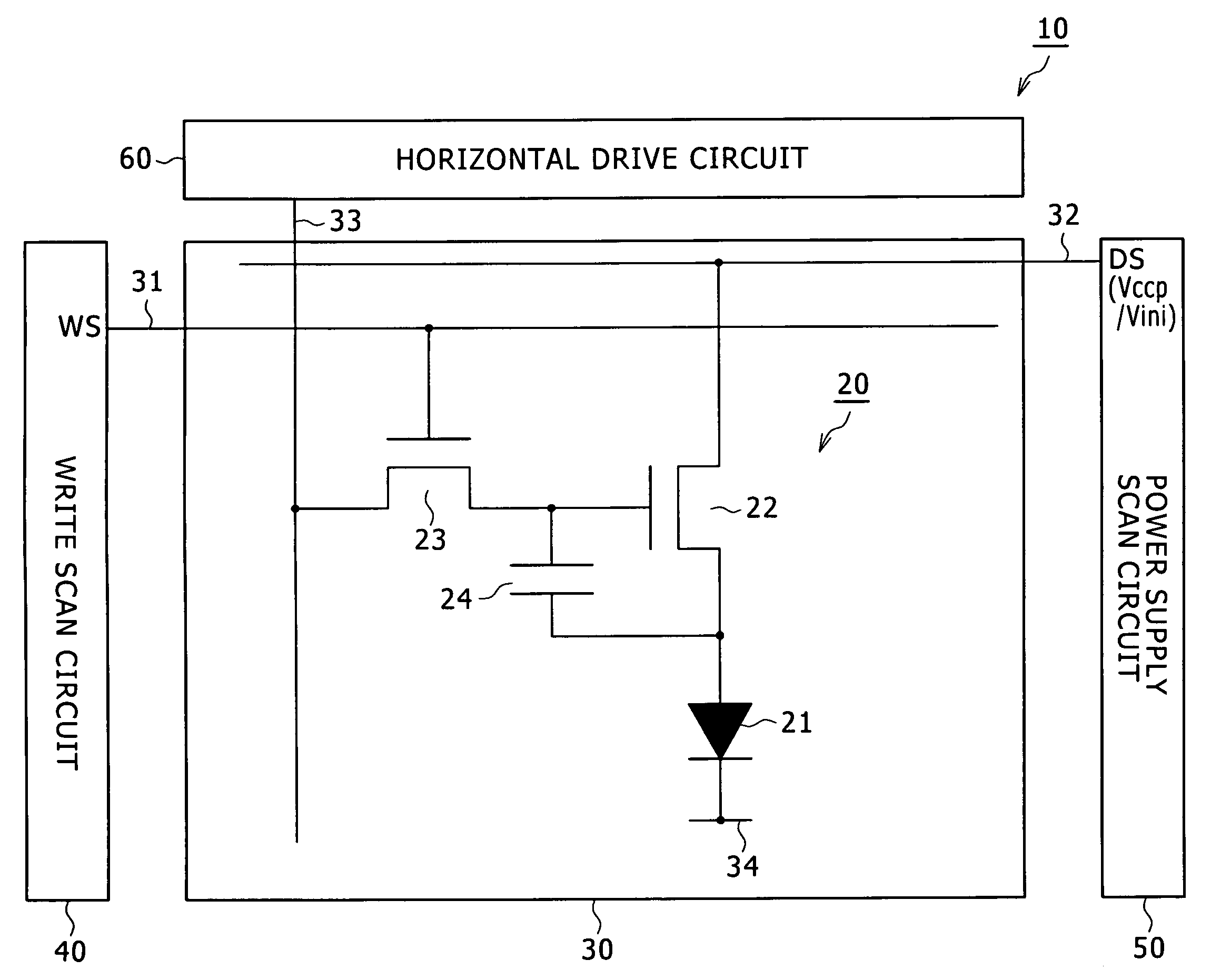
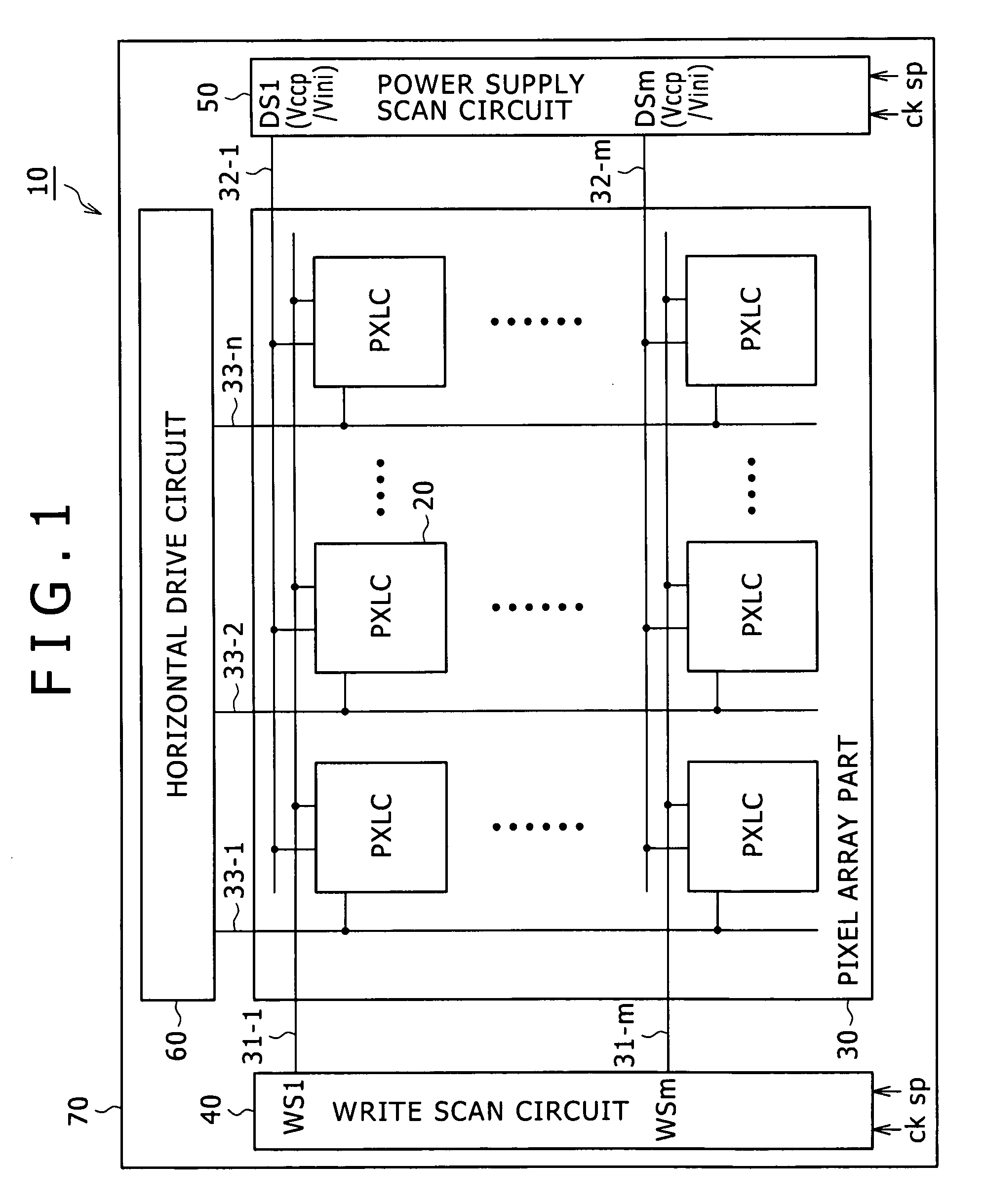
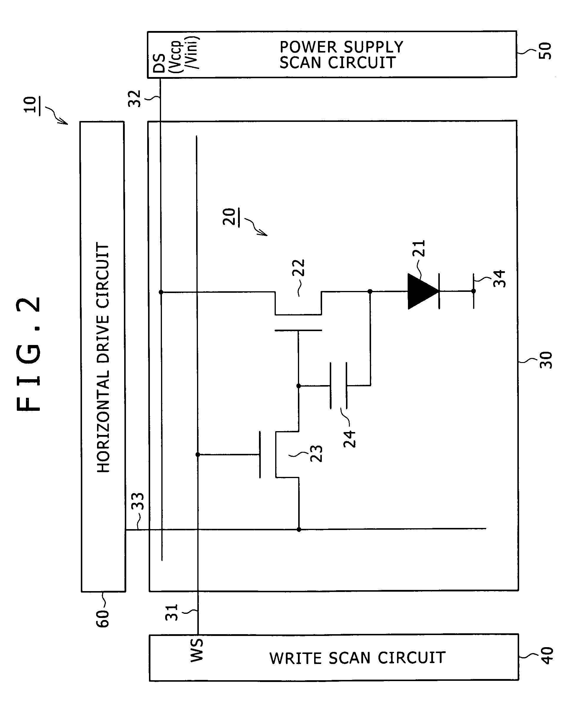
[0146]In the above-described embodiment, as an example, its feature is applied to the organic EL display 10 having the pixel circuit 20 with the circuit configuration that includes the drive transistor 22 for driving the organic EL element 21, the write transistor 23 for sampling the signal voltage Vsig of the video signal and writing it in the pixel, and the holding capacitor 24 that is connected between the gate and source of the drive transistor 22 and holds the signal voltage Vsig written by the write transistor 23. However, the present invention is not limited to this application example.

[0147]The embodiment can be similarly applied also to organic EL displays having any of the following pixel circuits: a pixel circuit having a switching transistor that is connected between the drive transistor 22 and a power supply line and operates to selectively supply drive current from the power supply line to the drive transistor 22; and a pixel circuit further having a switching transist...


PUM


Abstract

Disclosed herein is a display including: a pixel array part configured to include pixels that are arranged in a matrix, each having an electro-optical element, a write transistor for writing a video signal, a drive transistor for driving the electro-optical element based on the video signal written by the write transistor, and a holding capacitor connected between the gate and source of the drive transistor, wherein the holding capacitor includes a first electrode, a second electrode disposed to face one surface of the first electrode for forming a first capacitor, and a third electrode disposed to face the other surface of the first electrode for forming a second capacitor, and the first capacitor and the second capacitor are connected in parallel to each other electrically.

Description

CROSS REFERENCES TO RELATED APPLICATIONS[0001]The present invention contains subject matter related to Japanese Patent Application JP 2007-101282 filed in the Japan Patent Office on Apr. 9, 2007, the entire contents of which being incorporated herein by reference.BACKGROUND OF THE INVENTION[0002]1. Field of the Invention[0003]The present invention relates to a display, a method for driving a display, and electronic apparatus, and particularly to a flat-type (flat-panel) display in which pixels, each including an electro-optical element, are arranged on rows and columns (in a matrix), a method for driving the display, and electronic apparatus including the display.[0004]2. Description of the Related Art[0005]In recent years, in the field of displays for image displaying, flat-type display obtained by arranging pixels (pixel circuits) each including a light-emitting element in a matrix is prevailing rapidly. As the flat-type display, an organic electroluminescence (EL) display is bein...

Claims


Application Information

Patent Timeline
IPC IPC(8): H01J7/44H01J9/12
CPCG09G3/3233G09G3/3266G09G3/3291G09G2300/0819G09G2300/0842G09G3/3208G09G2310/0256G09G2320/043G09G2320/045H01L27/3265H01L27/3244G09G2300/0866H10K59/1216G09G3/20G09G3/30H05B33/12H10K50/00G09G5/10G09G2330/021H10K59/12H01L27/1222H01L27/1255
Inventor SAGAWA, HIROSHIUCHINO, KATSUHIDEYAMAMOTO, TETSURO
Owner SONY CORP
Why Eureka
Try Eureka