

Substrate Processing Apparatus and Reaction Container
a technology of substrate and processing apparatus, which is applied in the direction of coatings, chemical vapor deposition coatings, electric discharge tubes, etc., can solve the problems of adversely affecting the flow velocity of gas
- Summary
- Abstract
- Description
- Claims
- Application Information
AI Technical Summary
Benefits of technology
Problems solved by technology
Method used
Image

Examples
first embodiment
Embodiment Using CVD Method for Film Forming Process
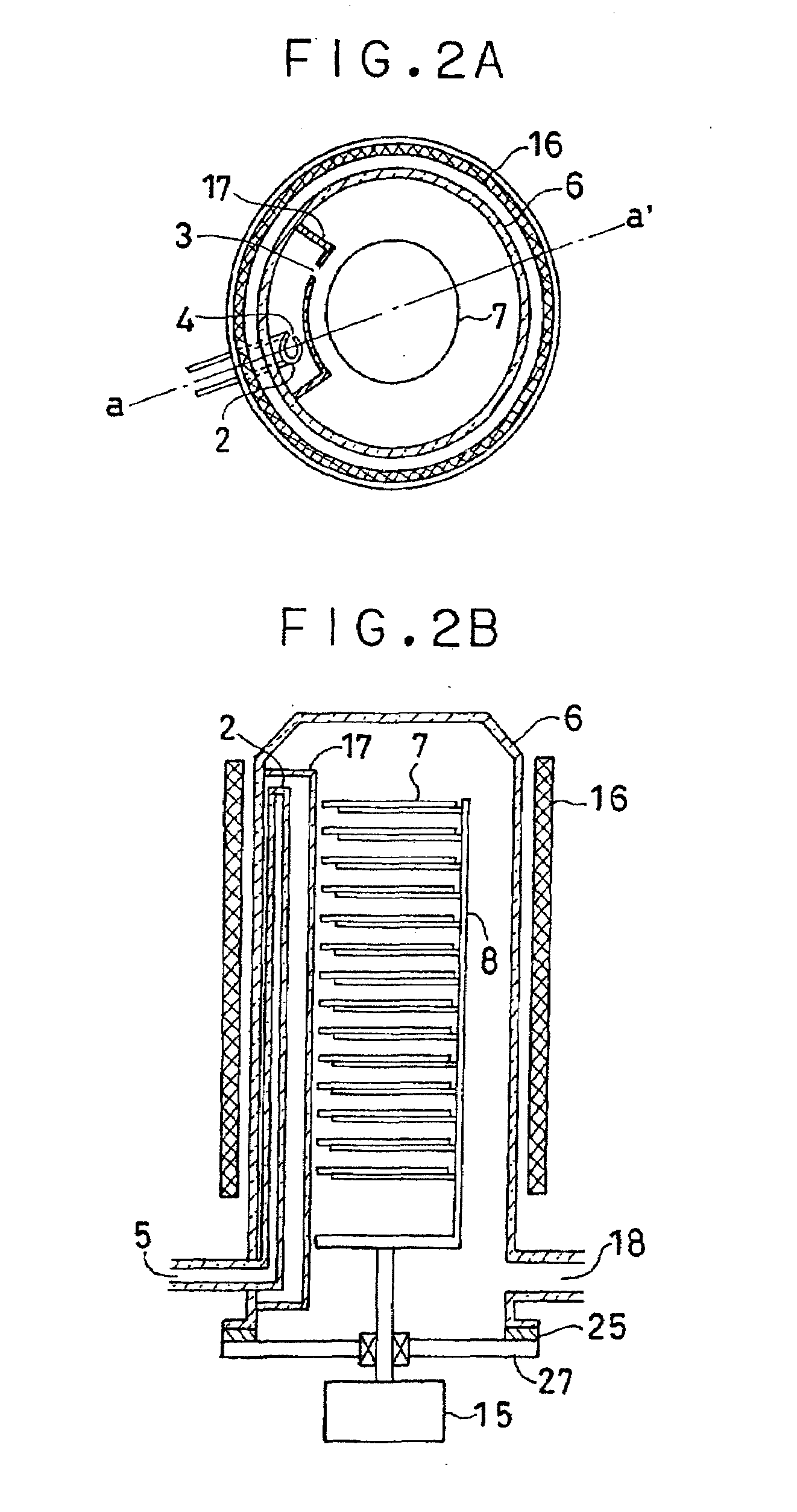
[0107]FIG. 2A is a schematic lateral sectional view of the reaction tube in the vertical type substrate processing apparatus according to this embodiment, and FIG. 2B is a vertical sectional view taken along a line a-a′ in FIG. 2A.
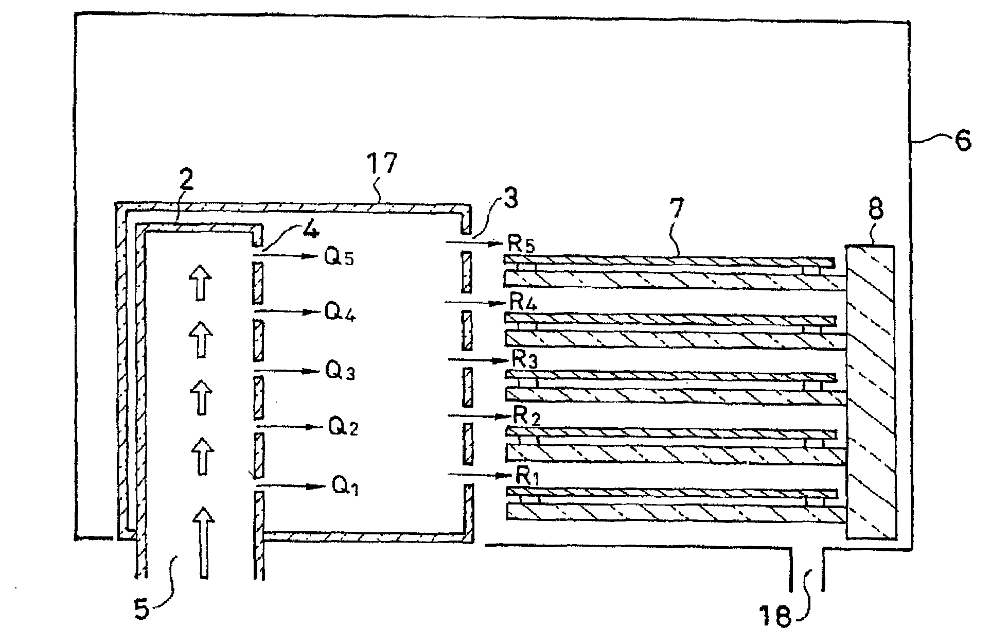
[0108]In FIG. 2A, a heater 16 is provided on an outer periphery of the reaction tube 6 which is a vertical type reaction chamber. A plurality of wafers 7 as substrates to be processed are stacked and placed in the reaction tube 6. In an arc space between the wafers 7 and an inner wall of the reaction tube 6, a buffer chamber 17 is provided on an inner wall of the reaction tube 6 from its lower portion to its upper portion along a stacking direction of the wafers 7. Buffer chamber holes 3 as gas-supply openings are provided in an end of a wall of the buffer chamber 17 which is adjacent to the wafer 7. The buffer chamber holes 3 are opened toward a center of the reaction tube 6.
[0109]An end of the buffer ch...
second embodiment
Embodiment Using ALD Method for Film Forming Process
[0135]An embodiment for forming films by the ALD method will be explained concretely.
[0136]When films are formed on the wafers 7 by the ALD method also, the above-described vertical type substrate processing apparatus can be used. In the case of the ALD method, however, if it is required to activate the processing gas by plasma or the like, an apparatus and an operation required for this process are added.
[0137]A case for forming films by the ALD method will be explained below using FIGS. 5A, 5B and 5C and FIG. 6.
[0138]FIGS. 5A, 5B and 5C show, from a side, an outward appearance and the inside of the reaction tube which is the reaction chamber in the vertical type substrate processing apparatus of the invention used for forming films by the ALD method. FIG. 6 is a lateral sectional view taken along a line A-A.
[0139]FIG. 5A shows the outward appearance of the reaction chamber. FIGS. 5B and C are vertical sectional views of the react...
fifth embodiments
Third to Fifth Embodiments
Different Embodiments Using ALD Method for Film Forming Process
[0186]FIG. 7 is a lateral sectional view of a reaction tube of a vertical type substrate processing apparatus according to a third embodiment of the present invention.
[0187]The reaction tube 6 shown in FIG. 7 has the same structure as that shown in FIG. 6. In FIG. 6, the electrode for producing plasma is disposed in the buffer chamber 17. In FIG. 7, an ultraviolet lamp 54 for activating gas and a reflection plate 58 for preventing ultraviolet from radiating out from the buffer chamber 17 are provided in combination.
[0188]Reaction gas is activated by light energy of the lamp 54.
[0189]The processing gas which is brought into the active species in the buffer chamber 17 having the above structure is injected toward the wafers 7 from the buffer chamber holes 3, and films are formed on the wafers 7 by the ALD method.
[0190]FIG. 8 is a lateral sectional view of a reaction tube of a vertical type substra...
PUM
| Property | Measurement | Unit |
|---|---|---|
| flow rate | aaaaa | aaaaa |
| flow velocity | aaaaa | aaaaa |
| flow rates | aaaaa | aaaaa |
Abstract
Description
Claims
Application Information