Light-emitting diode and method for producing it

a technology of light-emitting diodes and diodes, which is applied in the manufacture of printed circuits, solid-state devices, printed circuit assembling, etc., can solve the problems of reducing the light intensity due to the absorbed light of adjacent led elements on the side surfaces of adjacent led elements, and achieves enhanced emission efficiency and miniaturization

Inactive Publication Date: 2008-10-16
CITIZEN ELECTRONICS CO LTD
View PDF4 Cites 21 Cited by
  • Summary
  • Abstract
  • Description
  • Claims
  • Application Information

AI Technical Summary

Benefits of technology

[0014]An object of the present invention is to provide an LED capa

Problems solved by technology

In this way, if the plurality of LED elements are mounted and used, a part of laterally emitted light is absorbed in a side surface of

Method used


Image

  • Light-emitting diode and method for producing it
  • Light-emitting diode and method for producing it
  • Light-emitting diode and method for producing it

Examples


first embodiment

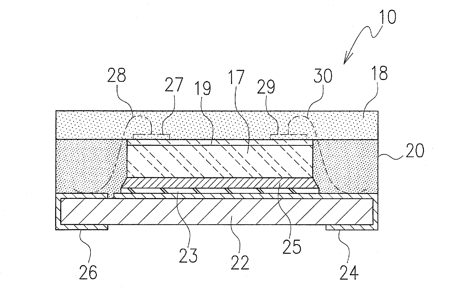
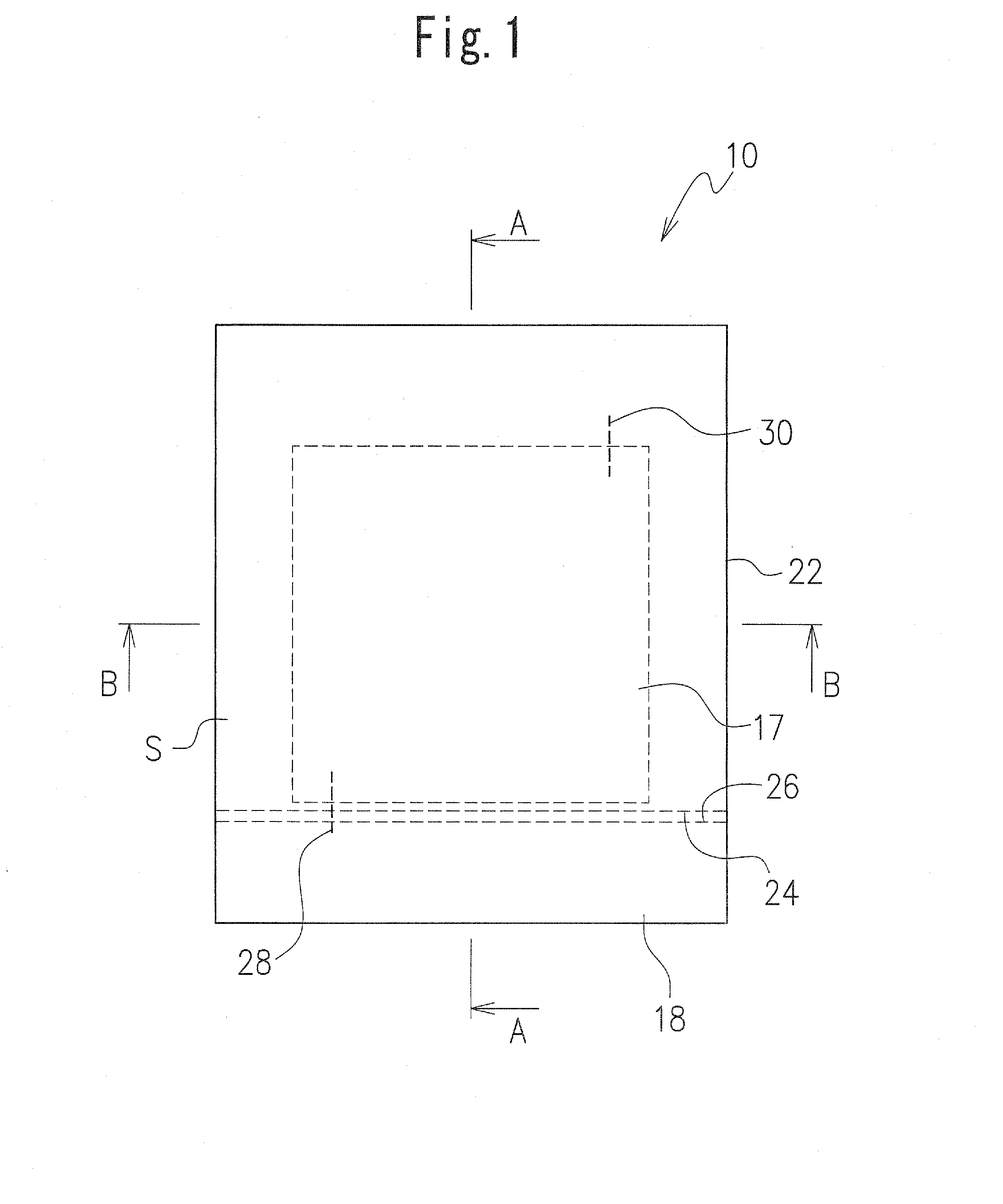
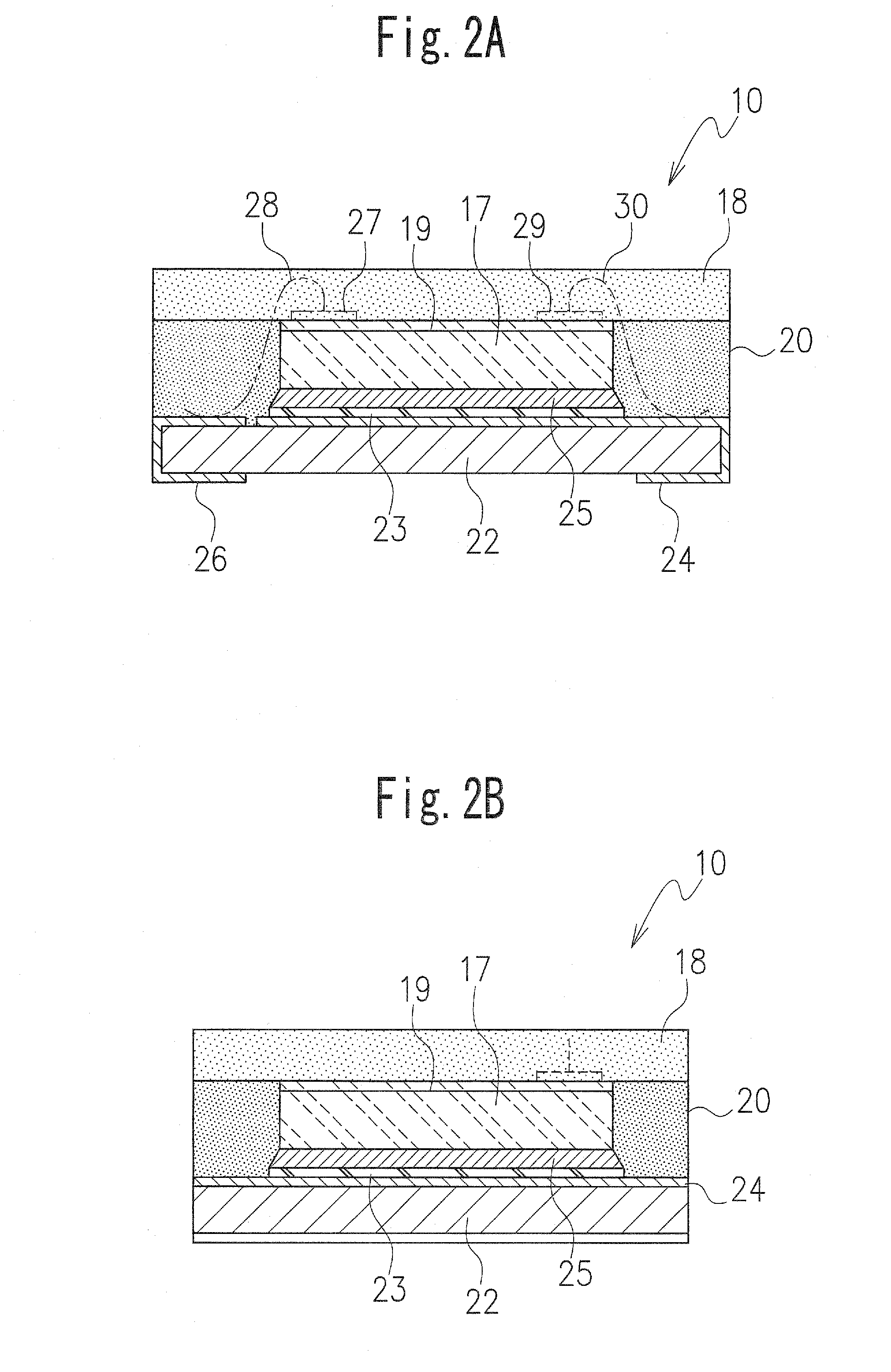
[0043]FIGS. 1, 2A, 2B and 3 illustrate an LED according to a first embodiment of the present invention.

[0044]The LED 10 in the first embodiment includes a board or printed circuit board 22 provided with electrodes 24 and 26, with at least one LED element 17 mounted on the board or printed circuit board 22 and electrically connected to the electrodes 24 and 26. Here, for example, an LED element is directly mounted on the electrode 24 (see FIGS. 1, 2A, 2B and 3). The printed circuit board 22 may be made of a resin, for example, and in the first embodiment has a rectangular shape and a certain size, and an outline of the LED element 17 here has a rectangular shape smaller than that of the printed circuit board 22 (see FIG. 1). The LED element 17 is disposed at a generally central portion of the printed circuit board 22, and therefore a space S is defined around side surfaces of the LED element 17 on an upper surface of the printed circuit board 22 (see FIG. 1).

[0045]As shown in FIG. 2A...

second embodiment

[0056]FIGS. 4, 5A, 5B and 6 illustrate an LED according to a second embodiment of the present invention. In the second embodiment, the same reference numbers are attached to parts which are the same as those in the first embodiment.

[0057]In the LED 31 according to the second embodiment, an LED element 44 is mounted on the printed circuit board 22 and electrically connected to electrodes 36 and 38 provided on the printed circuit board 22 by bumps 40 without using bonding wires (flip-chip system). Therefore, the LED in the second embodiment may be formed to have a size smaller than that according to the first embodiment. In a top plan view, outlines of the first sealing member 20, the second sealing member 18, and the printed circuit board are substantially same, and these configurations make it possible to shield lateral light from the LED element effectively, even as a smaller-sized LED.

[0058]Also, in the second embodiment, because it is not necessary to provide bonding wire portion...

third embodiment

[0060]FIGS. 7, 8A and 8B illustrate an LED according to a third embodiment of the present invention.

[0061]In the LED 50 in the third embodiment, three LED elements 52, 54 and 66 are mounted on the printed circuit board 22, as shown in FIGS. 7 and 8B. The LED elements 52, 54 and 56 are electrically connected through wires 16 to electrodes 64 and 66 provided on the printed circuit board 22 (see FIGS. 8A and 8B). A first sealing member 62 is disposed to surround side surfaces of each of the LED elements 52, 54 and 56, and a second sealing member 60 is disposed to cover a substantially flat surface composed of the upper surfaces of the LED elements 52, 54 and 56 and the first sealing member 62.


PUM

PropertyMeasurementUnit
Thermal conductivityaaaaaaaaaa

Abstract

An LED includes a printed circuit board, at least one LED element including a junction and mounted on the printed circuit board, a first sealing member disposed to cover side surfaces of the LED element, and a second sealing member disposed to cover side surfaces of the LED element. The first sealing member is configured to reflect and shield light emitted from the junction of the LED element, and the second sealing member is configured to transmit light emitted from the LED element.

Description

CROSS-REFERENCE TO THE RELATED APPLICATION[0001]This application is based on and claims priority from Japanese Patent Application No. 2007-087826, filed on Mar. 29, 2007, the disclosure of which is incorporated herein by reference in its entirety.BACKGROUND OF THE INVENTION[0002]1. Field of the Invention[0003]The present invention relates to a light-emitting diode (LED) and a method for producing such an LED.[0004]2. Description of Related Art[0005]For a conventional surface-mount-type LED, it has become more important to improve emission efficiency, to extend a life duration of an instrument using the LED, and to miniaturize the LED. There also has been a requirement for a method to produce an LED inexpensively.[0006]FIGS. 17A and 17B illustrate conventional surface-mount type-LEDs, respectively.[0007]The LED 100 shown in FIG. 17A includes a board 112 provided with a pair of electrodes 114 and 116, an LED element 106 mounted on, for example, the electrode 114 and a transparent seal...

Claims


Application Information

Patent Timeline
IPC IPC(8): H05K1/00H05K3/30H01L33/62H01L33/56
CPCH01L33/54Y10T29/4913H01L33/60H01L2924/3025H01L33/56H01L2224/32225H01L2224/16225H01L2224/8592H01L24/48H01L24/97H01L2224/48091H01L2924/00014H01L2924/00H01L2924/12041H01L2924/181H01L2924/00011H01L2224/45099H01L2224/05599H01L2924/00012H01L2224/0401
Inventor KADOTANI, NORIKAZUNISHIDA, ATSUSHIFUKASAWA, KOICHIISHII, HIROHIKO
Owner CITIZEN ELECTRONICS CO LTD
Why Eureka
Try Eureka