

Integrated opc verification tool
a verification tool and integrated technology, applied in the field of integrated device layout design tools, can solve the problems of data loss, inaccurate translation, time-consuming, etc., and achieve the effect of reducing the cost of vlsi ics
- Summary
- Abstract
- Description
- Claims
- Application Information
AI Technical Summary
Benefits of technology
Problems solved by technology
Method used
Image

Examples
Embodiment Construction
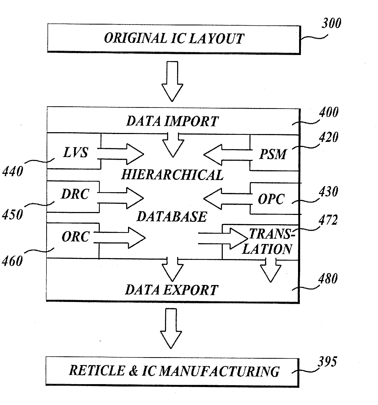
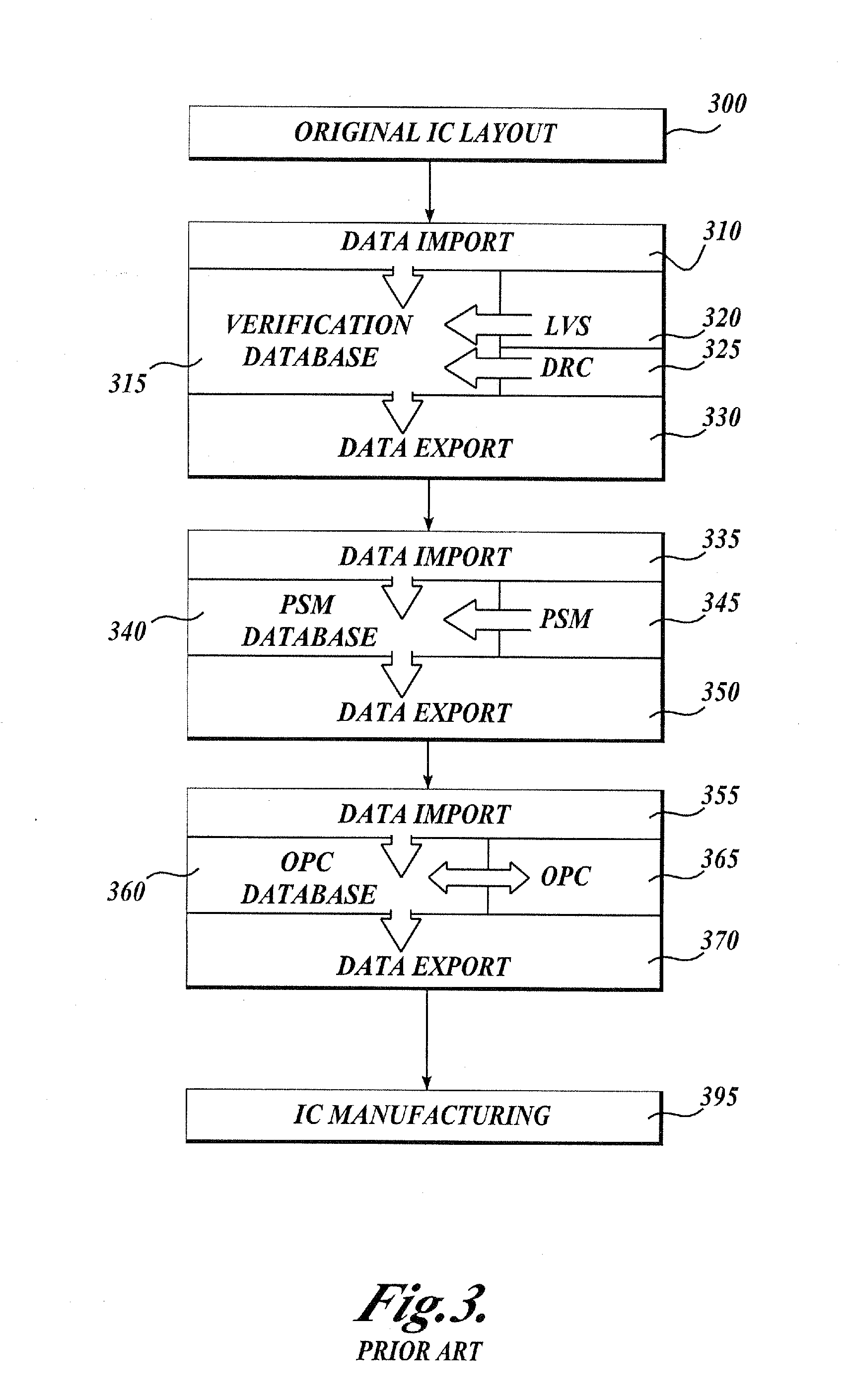
[0028]An integrated verification and manufacturability tool is described. In the following description, for purposes of explanation, numerous specific details are set forth in order to provide a thorough understanding of the invention. It will be apparent, however, to one skilled in the art that the invention can be practiced without these specific details. In other instances, structures and devices are shown in block diagram form in order to avoid obscuring the invention.
[0029]Reference in the specification to “one embodiment” or “an embodiment” means that a particular feature, structure, or characteristic described in connection with the embodiment is included in at least one embodiment of the invention. The appearances of the phrase “in one embodiment” in various places in the specification are not necessarily all referring to the same embodiment.
[0030]Methods and apparatuses are described herein with respect to integrated circuit manufacturing; however, the techniques described ...
PUM
| Property | Measurement | Unit |
|---|---|---|
| transmission | aaaaa | aaaaa |
| physical layout | aaaaa | aaaaa |
| dimensions | aaaaa | aaaaa |
Abstract
Description
Claims
Application Information