Method of manufacturing inductor

Active Publication Date: 2008-10-23
MURATA MFG CO LTD
View PDF4 Cites 69 Cited by
  • Summary
  • Abstract
  • Description
  • Claims
  • Application Information

AI Technical Summary

Benefits of technology

[0009]To overcome the problems described above, preferred embodiments of the present invention provide a method of manufacturing an inductor capable of effectively utili

Problems solved by technology

However, the above-described manufacturing method of the related art has the following problems.
For this reason, the size of the chip 100A is reduc

Method used


Image

  • Method of manufacturing inductor
  • Method of manufacturing inductor
  • Method of manufacturing inductor

Examples


first preferred embodiment

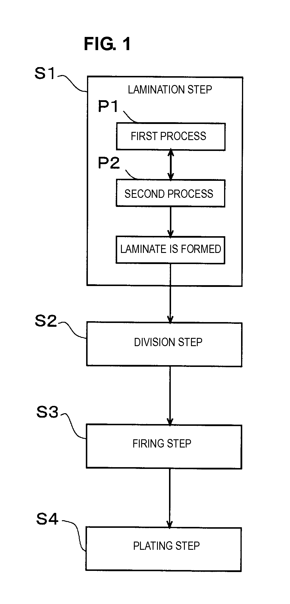
[0055]FIG. 1 is a block diagram showing a method of manufacturing an inductor according to a first preferred embodiment of the present invention.

[0056]As shown in FIG. 1, a method of manufacturing an inductor according to this preferred embodiment includes a lamination step S1, a division step S2, a firing step S3, and a plating step S4. Then, the lamination step S1 includes a first process P1 and a second process P2, and by repeatedly performing the first and second processes P1 and P2, a laminate of inductors is formed.

[0057]Here, in order to facilitate understanding of the method of manufacturing an inductor according to this preferred embodiment, the configuration of an inductor manufactured in this preferred embodiment will be described in advance.

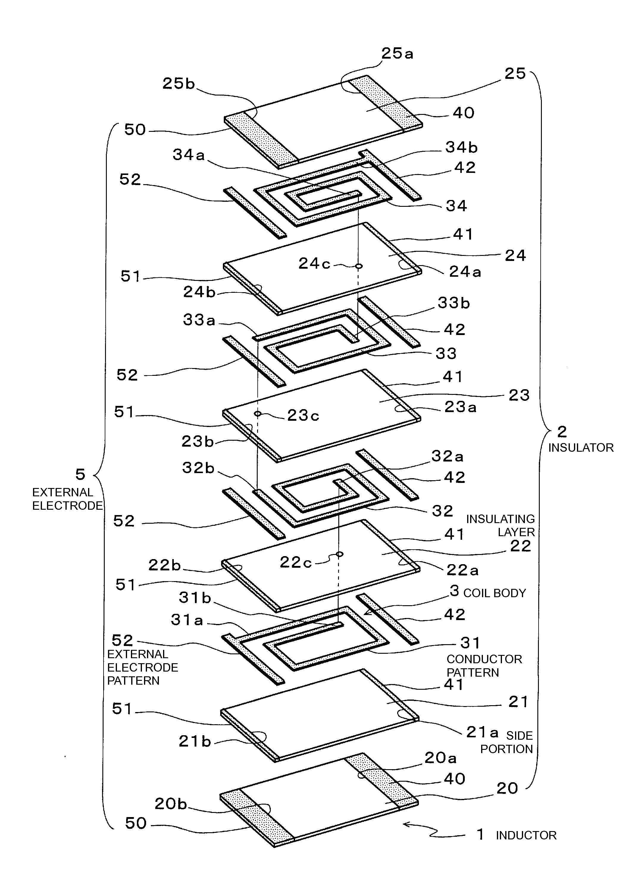
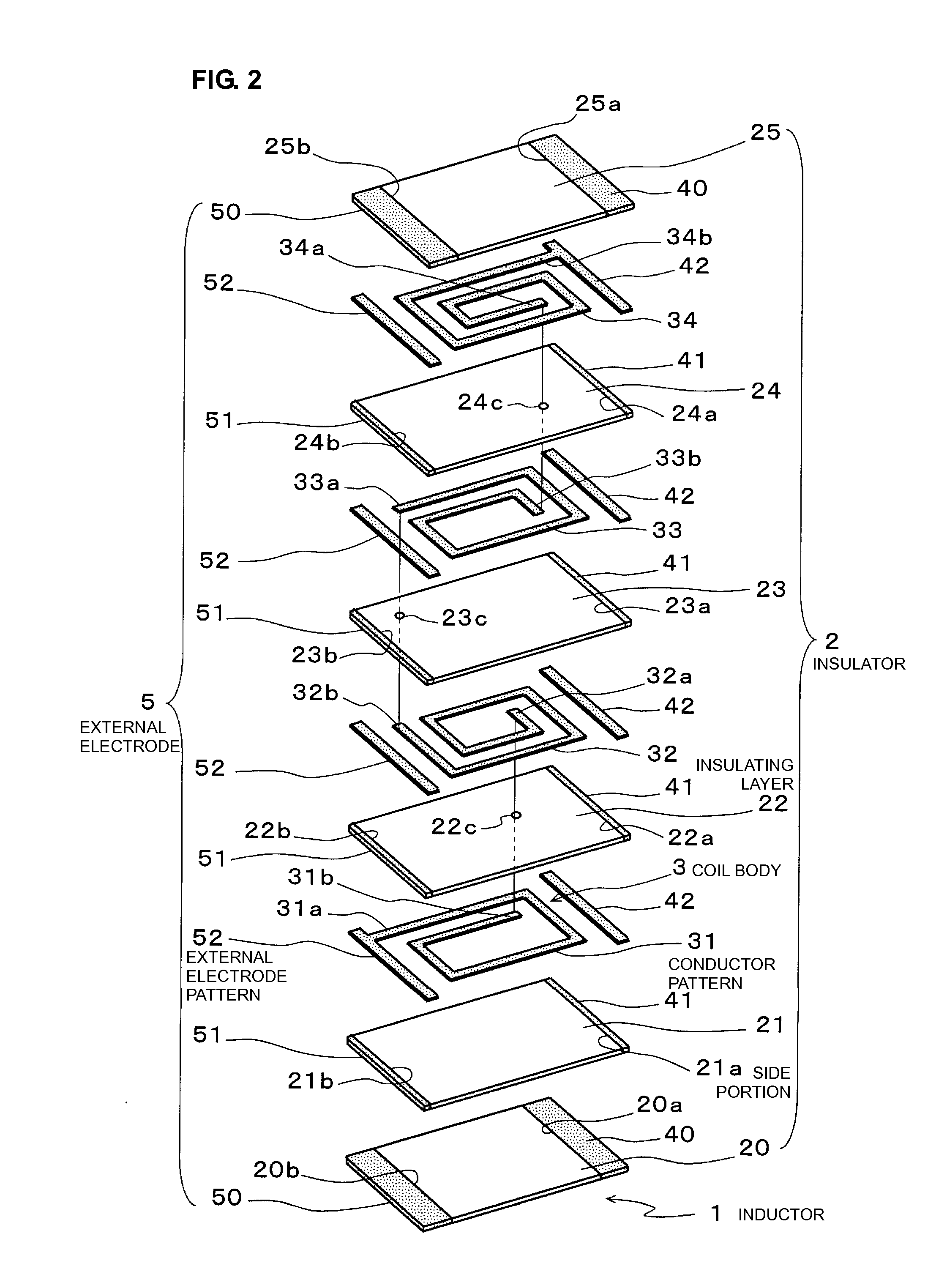
[0058]FIG. 2 is an exploded perspective view of an inductor. FIG. 3 is a perspective view of an inductor in a state in which a coil body is shown transparently. FIG. 4 is a sectional view taken along the line A-A in FIG. 3.

[0059]As sh...

second preferred embodiment

[0103]Next, a second preferred embodiment of the present invention will be described.

[0104]FIG. 12 is an exploded perspective view of an inductor manufactured using a method according to the second preferred embodiment of the present invention. FIG. 13 is a perspective view of an inductor in a state in which a coil body is shown transparently.

[0105]This preferred embodiment is a method of manufacturing an inductor 1′ having external electrodes 4′ and 5′, which are L-shaped when viewed from the lamination direction, as shown in FIG. 13.

[0106]That is, in the second process P2 of the lamination step S1, as shown in FIG. 12, L-shaped cutout portions 20a′ and 20b′ are formed in both corner portions (corner portions on both right and left sides in the figure) of one side portion 20d of the insulating layer 20, and wide filling conductors 40′ and 50′ are formed in these cutout portions 20a′ and 20b′, respectively. Furthermore, on the topmost insulating layer 25, similarly, L-shaped cutout ...

third preferred embodiment

[0124]Next, a third preferred embodiment of the present invention will be described.

[0125]FIG. 18 is an exploded perspective view of an inductor manufactured by the method of the third preferred embodiment of the present invention. FIG. 19 is a perspective view of an inductor in a state in which a coil body is shown transparently. FIG. 20 is a perspective view showing a state in which an inductor is mounted.

[0126]This preferred embodiment, as shown in FIG. 19, is a method of manufacturing an inductor 1″ having external electrodes 4″ and 5″ formed in a long shape when viewed from the lamination direction in two corner portions.

[0127]That is, as shown in FIG. 18, wide filling conductors 40″ and 50″ having an elongated shape, which are shorter than half the length of the side portion 20d (25d), are formed in two corner portions of one side portion 20d (25) of the insulating layer 20, and narrow filling conductors 41″ and 51″ having substantially the same length are formed in the two co...


PUM

PropertyMeasurementUnit
Lengthaaaaaaaaaa
Shapeaaaaaaaaaa
Electrical conductoraaaaaaaaaa

Abstract

A method of manufacturing an inductor includes a lamination step, a division step, a firing step, and a plating step. In the lamination step, a laminate including an insulator, a coil body, and external electrodes is formed. That is, in the lamination step, insulating layers having wide filling conductors, insulating layers having narrow filling conductors, and conductor patterns having external electrode patterns are laminated. As a result, the conductor patterns form the coil body, and the wide filling conductors, the narrow filling conductors, and the external electrode patterns form the external electrodes. The narrow filling conductors have a width that is less than the widths of the wide filling conductors and the external electrode patterns, and recesses and projections are provided in the external electrodes.

Description

BACKGROUND OF THE INVENTION[0001]1. Field of the Invention[0002]The present invention relates to a method of manufacturing an inductor preferably for use in a mobile phone, for example.[0003]2. Description of the Related Art Japanese Unexamined Patent Application Publication No. 11-204336 and Japanese Unexamined Patent Application Publication No. 2005-109097 disclose methods of manufacturing an inductor.[0004]According to a manufacturing method of the related art, PET films and dummy substrates are used as base materials, and a photosensitive insulating paste is printed on the base material. Then, the photosensitive insulating paste is exposed (developed and additionally exposed as necessary) and dried to form an insulating layer. The photosensitive conductive paste is printed, exposed, developed (additionally exposed as necessary), and dried to form a conductor pattern. Next, the photosensitive insulating paste is printed, exposed, developed (additionally exposed as necessary), and...

Claims


Application Information

Patent Timeline
IPC IPC(8): B32B37/02B32B38/14
CPCH01F17/0013H01F27/292H01F41/041H01F2017/0073H01F41/122H01F27/306Y10T29/49078H03H2001/0078Y10T29/49073Y10T29/49147Y10T29/49155Y10T29/4902H03H2001/0085H03H7/0115H01F41/00
Inventor YAMANO, KAZUHIKO
Owner MURATA MFG CO LTD
Why Eureka
Try Eureka