Exposure device

a technology of exposure device and exposure process, which is applied in the direction of optical radiation measurement, instruments, photomechanical equipment, etc., can solve the problems of difficult preparation, exchange or maintenance, and the reaction speed of typical direct exposure device in forming pattern is low, and achieves stable exposure process and monitors the age deterioration of optical sources.

Inactive Publication Date: 2008-10-23
ORC MFG
View PDF3 Cites 14 Cited by
  • Summary
  • Abstract
  • Description
  • Claims
  • Application Information

AI Technical Summary

Benefits of technology

[0027]This structure is fabricated and maintained easily.
[0028]In the exposure device of the present invention, the ray(s) from light source(s) is / are split into multiple light beams by the aperture members, the intensity of the ray(s) is detected, and the operations of the spatial light modulators, the electric power supplied to the optical source(s), etc. are controlled properly based on the detected intensity. If provided with the two optical sources, then the exposure device adjusts the intensities of both optical sources, and monitors the age deterioration of the optical sources. In conclusion, with the exposure device of the present invention, proper and stable exposure process can be executed.

Problems solved by technology

However, those masks are hard to prepare, exchange or maintain, thus making it difficult to treat many different substrates efficiently.
However, a typical direct type exposure device tends to have a low reaction speed in forming patterns, because its light source is a laser of short wavelength such as 405 nm.
Hence, this property may cause the deterioration of the production capacity.
In addition to the low production capacity, a typical direct exposure device involves a cost increase.
If high-intensity light beams are irradiated to those many spatial light modulation elements, then many light sources are required, thus leading to the increase in the material costs.

Method used


Image

  • Exposure device
  • Exposure device
  • Exposure device

Examples


Embodiment Construction

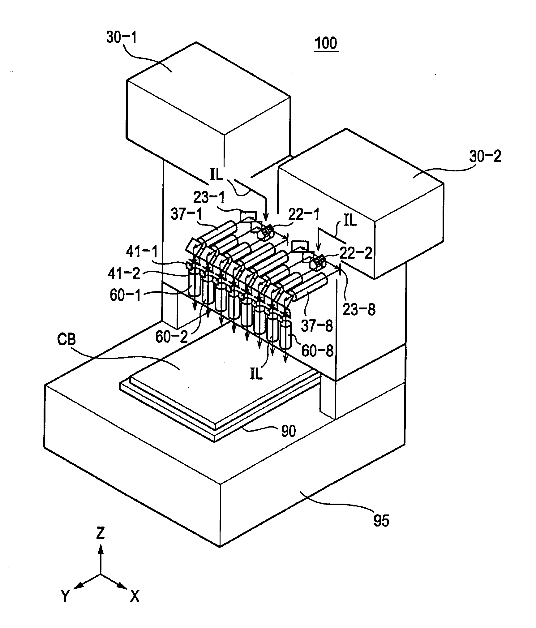
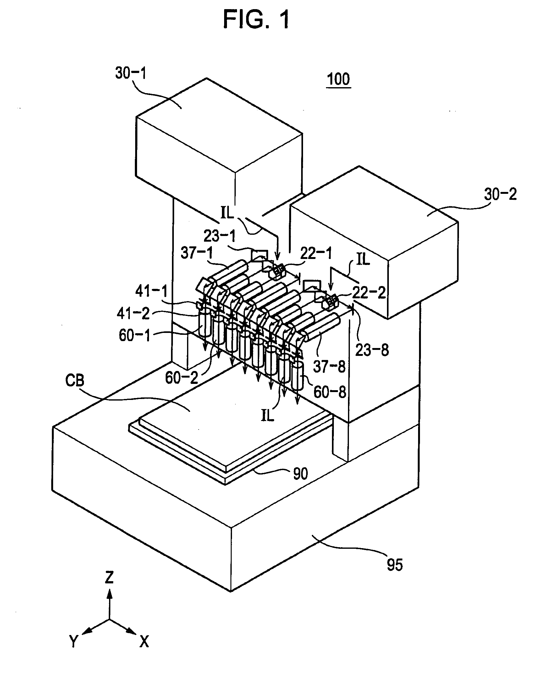
[0045]FIG. 1 schematically shows an exposure device 100 according to an embodiment of the present invention. This exposure device 100 mainly includes first lighting systems 30-1 and 30-2, second lighting systems 37-1 to 37-8, spatial light modulation systems (thereinafter referred to as “DMDs”) 41-1 to 41-8, projection optical systems 60-1 to 60-8, and an object table 90. The reason why the two first lighting systems (30-1 and 30-2) are used is to irradiate an object CB widely. These first lighting systems 30-1 and 30-2 contain a first high-pressure mercury lamp 10-1 and a second high-pressure mercury lamp 10-2 (see FIG. 2), respectively.

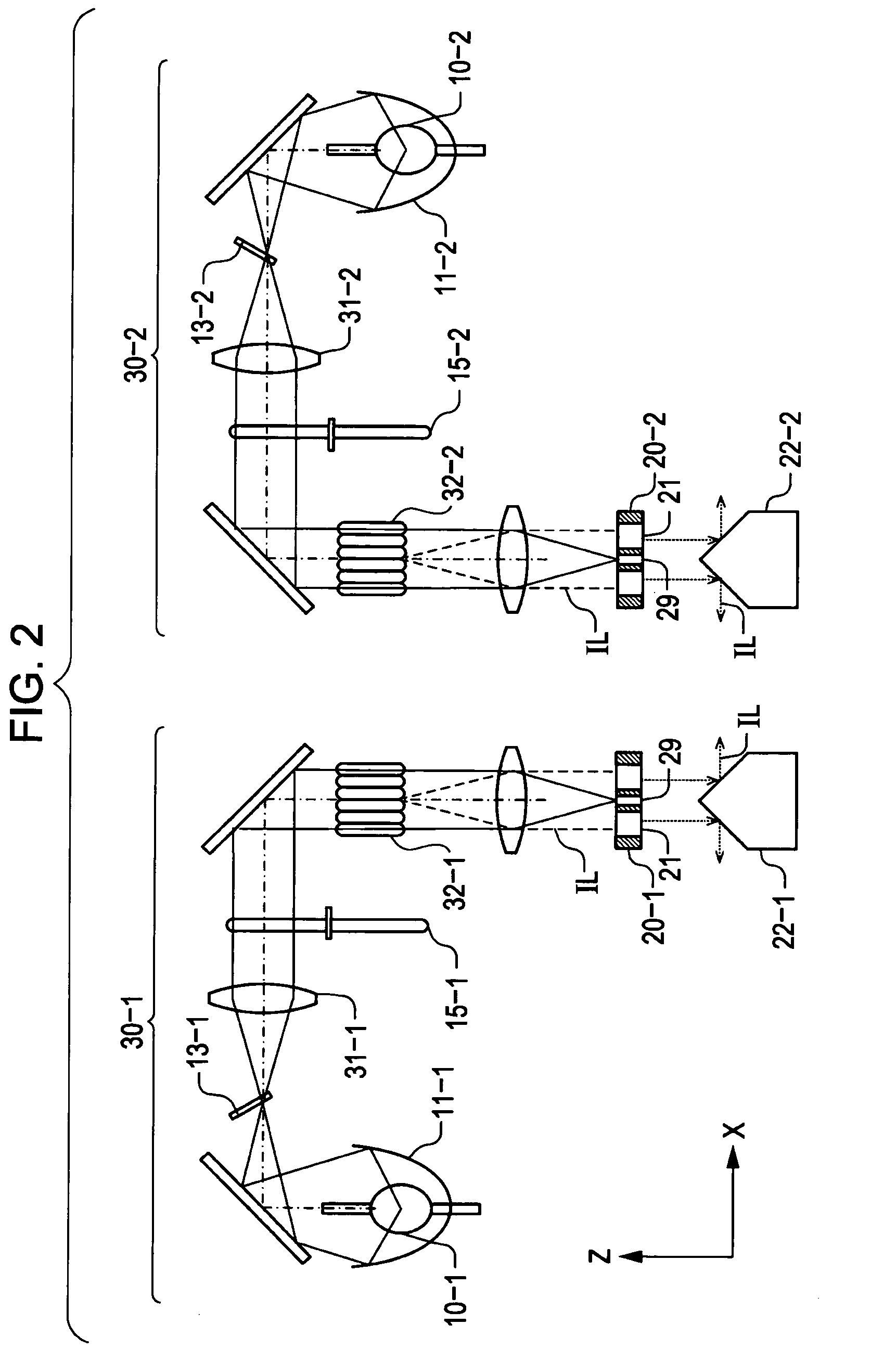
[0046]FIG. 2 schematically shows the first lighting systems 30-1 and 30-2. Since both lighting systems have the identical structure, only the first lighting system 30-1 will be described below.

[0047]In this drawing, the first high-pressure mercury lamp 10-1 is located at a primary focal point of an elliptic mirror 11-1. The elliptic mirror 11-1 refl...


PUM


Abstract

The present invention relates to an exposure device for forming predetermined patterns onto an object. The exposure device includes an optical source for emitting a ray, an aperture member including first and second opening windows and a detection window, first and second reflective optical elements for reflecting the first and second light beams that have passed through the first and second opening windows, respectively, and an optical sensor for detecting intensity of the ray from the optical source which has passed through the detection window, the optical sensor being placed close to an area between the first and second reflective optical elements.

Description

CROSS-REFERENCE TO RELATED APPLICATIONS[0001]This application claims the benefit of Japanese Patent Application 2007-083881 filed on Mar. 28, 2007, the disclosure of which is incorporated herein by reference.BACKGROUND OF THE INVENTION[0002]1. Field of the Invention[0003]The present invention relates to an exposure device for forming patterns on a surface of a flat-sheet material, including a substrate for an electronic circuit, a glass substrate for an LCD and a glass element substrate for a PDP.[0004]2. Description of the Related Art[0005]In general, substrates for electronic circuits or printed circuits are applied to electronic instruments such as portable phones or various types of PCs. On a substrate of this type, multiple fine patterns, lands and via-holes tend to be formed with great precision. In addition, an exposure device which forms such miniature patterns is required to handle many different types of substrates in a short period. In order to follow the trend as well as...

Claims


Application Information

Patent Timeline
Patent Type & Authority Applications(United States)
IPC IPC(8): G01J1/42
CPCG03F7/70275G03F7/70291
Inventor NONAKA, JUNLEE, DUKKOBAYASHI, YOSHINORI
Owner ORC MFG
Why Eureka
Try Eureka