Semiconductor Device and Method of Fabricating the Same

a technology of semiconductor devices and semiconductors, applied in the direction of semiconductor devices, basic electric elements, electrical equipment, etc., can solve the problem that the power trench mos transistor cannot be easily provided on the same chip, and the power trench mos transistor cannot be easily provided

Active Publication Date: 2008-10-23
MARVELL ASIA PTE LTD
View PDF24 Cites 20 Cited by
  • Summary
  • Abstract
  • Description
  • Claims
  • Application Information

AI Technical Summary

Problems solved by technology

However, the structure of the above described power trench MOS transistor does not easily provide a power trench MOS transistor on the same chip as a MOS transistor.

Method used


Image

  • Semiconductor Device and Method of Fabricating the Same
  • Semiconductor Device and Method of Fabricating the Same
  • Semiconductor Device and Method of Fabricating the Same

Examples


Embodiment Construction

[0014]A semiconductor device and a method of fabricating the semiconductor device will now be described with reference to the accompanying drawings according to embodiments.

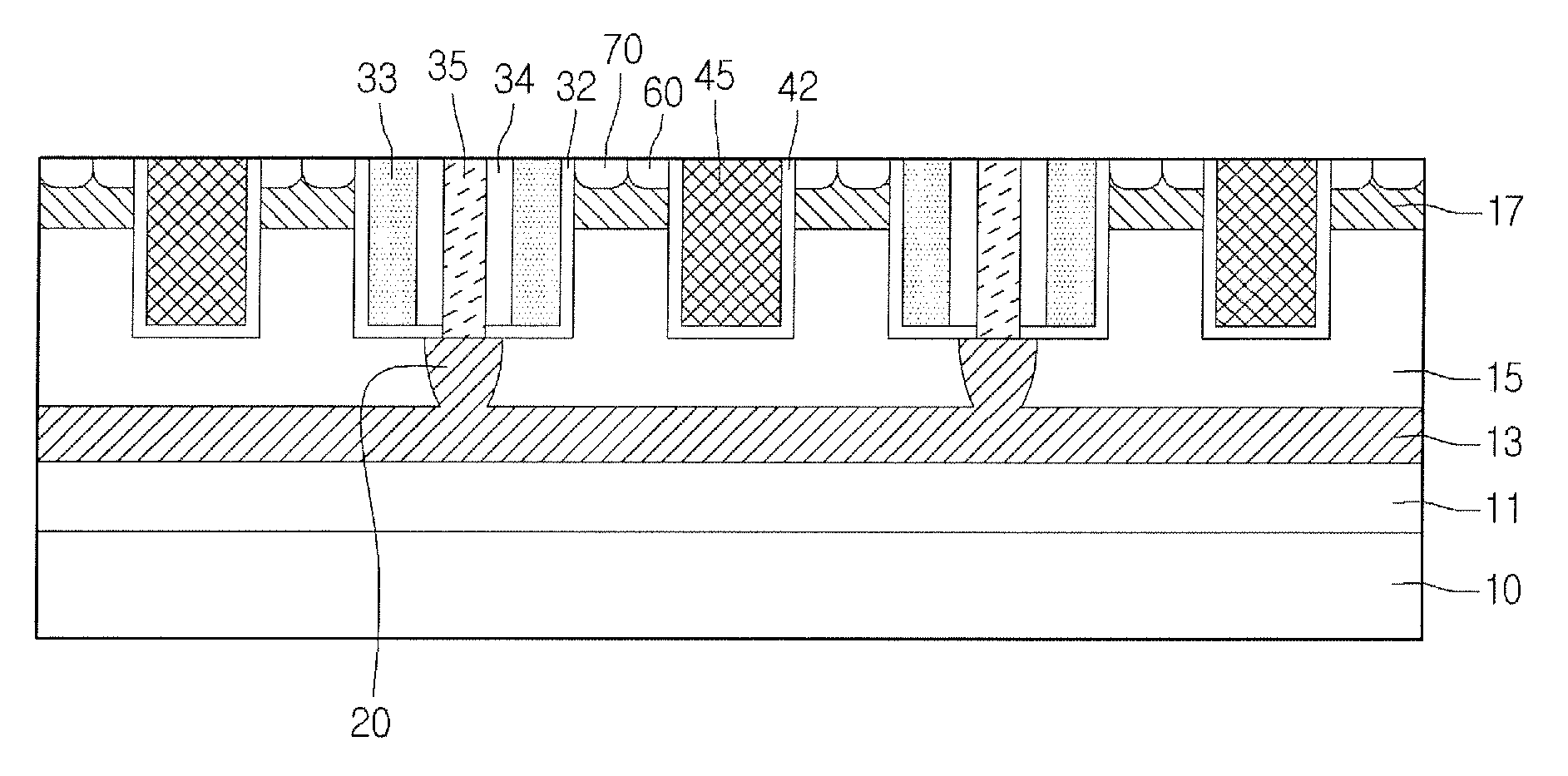
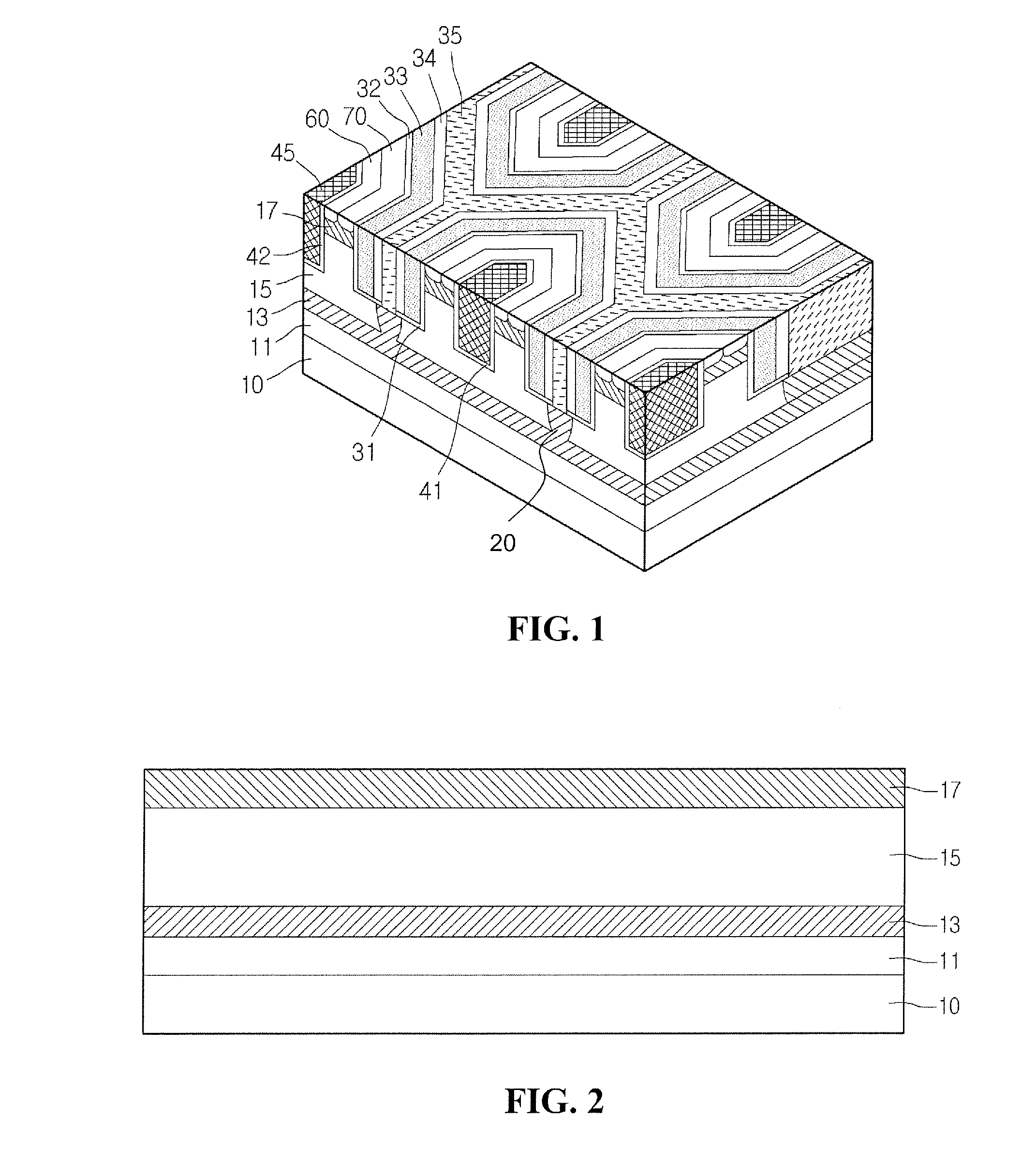
[0015]FIG. 1 is a view of a semiconductor device according to an embodiment.

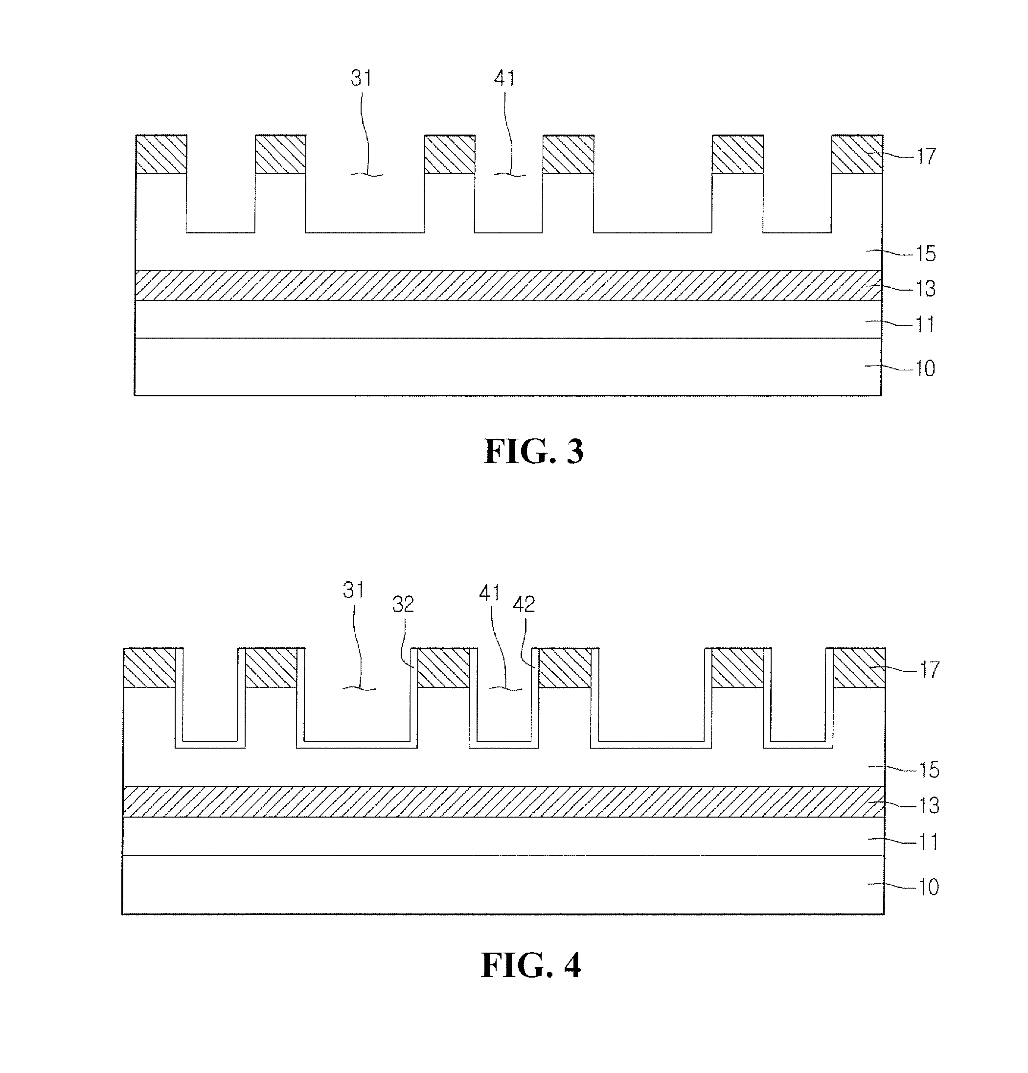
[0016]Referring to FIG. 1, a semiconductor device according an embodiment includes a first conductive type deep well 15, a second conductive type shallow well 17, a plurality of gate electrodes 45, a source region 60, a second conductive type body region 70, and a common drain 35. The first conductive type deep well 15 is disposed on a semiconductor substrate 10. The second conductive type shallow well 17 is disposed on the first conductive type deep well 15. The plurality of gate electrodes 45 can be formed in trenches 41 provided by selective removal of portions of the second conductive shallow well 17 and the first conductive type deep well 15. A gate dielectric 42 is disposed between the gate electrode 45 and the walls of the trench 4...


PUM


Abstract

Provided are a semiconductor device and a method of fabricating the semiconductor device. The semiconductor device can provide a trench MOS transistor having an up-drain structure. The semiconductor device can include a first conductive type well in a semiconductor substrate, a second conductive type well on the first conductive type well, trenches formed by removing portions of the second conductive type well and the first conductive type well; gates provided in the trenches with a gate dielectric being between each gate and the walls of the trench, a first conductive type source region and a second conductive type body region on the second conductive type well, the first conductive type source region surrounding a lateral surface of the gate, and a common drain between the gates, the common drain being connected to the first conductive type well.

Description

CROSS-REFERENCE TO RELATED APPLICATION[0001]The present application claims the benefit under 35 U.S.C. §119 of Korean Patent Application No. 10-2007-0037355, filed Apr. 17, 2007, which is hereby incorporated by reference in its entirety.BACKGROUND[0002]A trench-type metal-oxide-semiconductor (Trench MOS) transistor can be used as a power transistor.[0003]The power trench MOS transistor distinctly differs from a typical MOS transistor in that a channel of the power trench MOS transistor is formed in a vertical direction, not a horizontal direction.[0004]The power trench MOS transistor includes a vertical channel and a drain formed in a backside of a wafer as an output region.[0005]The power trench MOS transistor is suitable for high-current and high-voltage operation using a small area. To apply a high voltage to the power trench MOS transistor, a lightly doped drain region (a drift region) is formed to a sufficiently large length.[0006]Since electrons move vertically in the power tr...

Claims


Application Information

Patent Timeline
Patent Type & Authority Applications(United States)
IPC IPC(8): H01L29/00H01L21/8236
CPCH01L29/0653H01L29/0696H01L29/41766H01L29/4238H01L29/66719H01L29/66734H01L29/7809H01L29/7813
Inventor JANG, BYUNG TAK
Owner MARVELL ASIA PTE LTD
Why Eureka
Try Eureka