
Amorphous silicon photovoltaic cells having improved light trapping and electricity-generating method

a photovoltaic cell and amorphous silicon technology, applied in the direction of basic electric elements, electrical equipment, semiconductor devices, etc., can solve the problems of easy corrosion of silver, high cost of silicon thick layer,

Inactive Publication Date: 2008-10-30
FOREFRONT INNOVATIVE TECH
View PDF2 Cites 24 Cited by
  • Summary
  • Abstract
  • Description
  • Claims
  • Application Information

AI Technical Summary

Benefits of technology

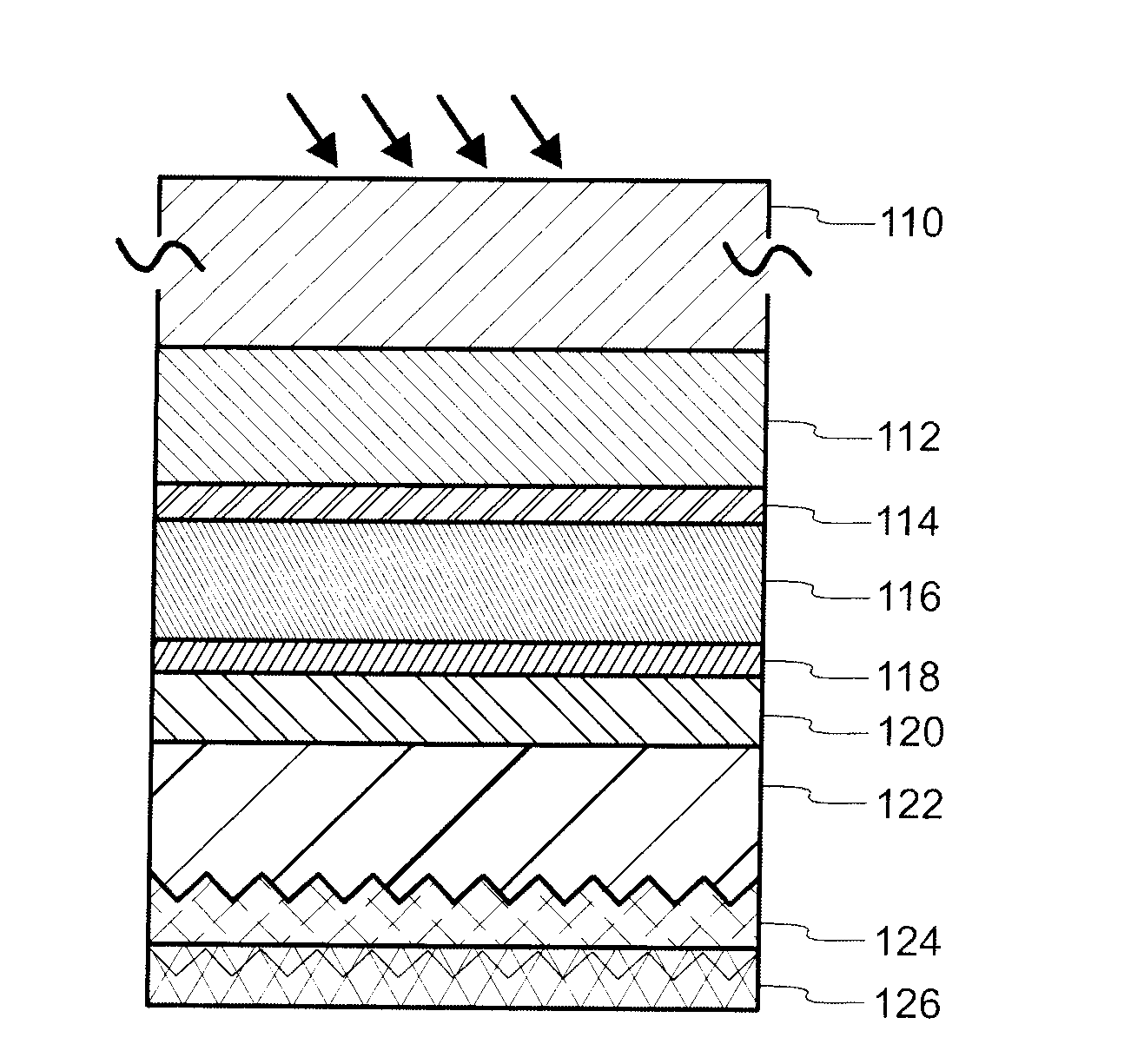
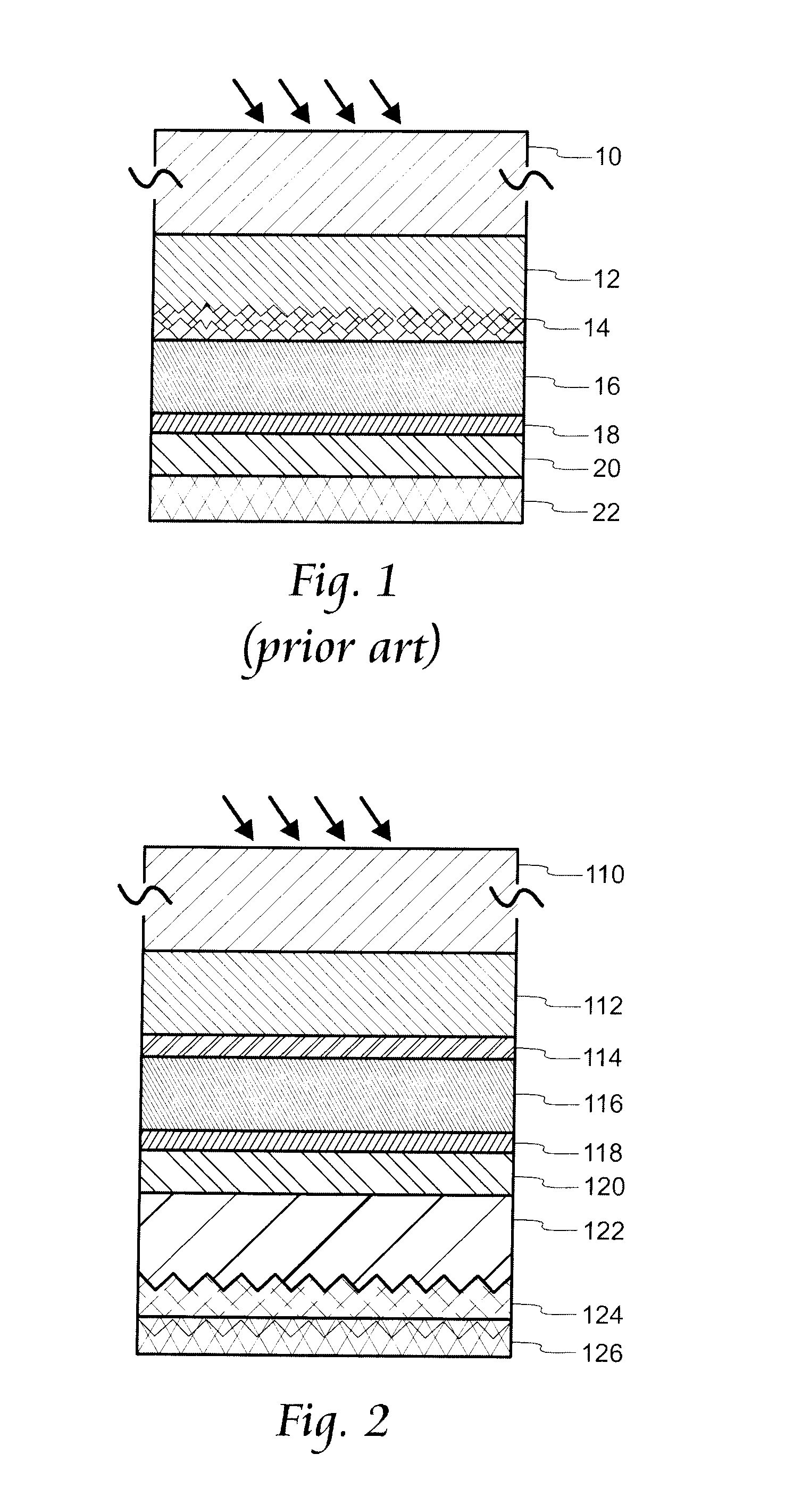
[0009]In accordance with a further embodiment of the present invention, a method for converting sunlight into electricity is disclosed. The method comprises: providing a photovoltaic cell comprising, in combination: a transparent superstrate; a first transparent conductor positioned below the transparent superstrate; wherein the first transparent conductor has specular transmission properties and causes minimal scattering of the light; at least one p-i-n structure having an active layer positioned below the first transparent conductor; a second transparent conductor positioned below the at least one p-i-n structure; and a layer of transparent material positioned below the second transparent conductor; positioning the photovoltaic cell so that sunlight may enter the transparent superstrate and thereafter pass through the active layer of the at least one p-i-n structure, where a portion of the sunlight is converted into electricity; and outputting the electricity from the photovoltaic cell.

Problems solved by technology

However, the cost of this thick layer of silicon is high, and the process for creating a solar cell with a thick layer can be expensive.
However, silver is expensive and it is easily corroded in outdoor environments.
Finally, the amount of texture in SnO2 transparent conductor can be difficult to control.
Too much texture will scatter too much light and prevent light from entering the cell.

Method used


Image

  • Amorphous silicon photovoltaic cells having improved light trapping and electricity-generating method
  • Amorphous silicon photovoltaic cells having improved light trapping and electricity-generating method

Examples


Embodiment Construction

[0012]Referring to FIG. 2, an amorphous silicon thin-film photovoltaic cell (hereinafter “cell”) consistent with an embodiment of the present invention is illustrated. The cell comprises multiple layers. These include a transparent superstrate 110, which may be glass or another transparent material. Next in the cell of FIG. 2 is a layer of a transparent conductor 112 such as SnO2 or ZnO. As noted above, in the prior art, this layer is often textured to scatter approximately 10 to 15% of the incoming light so that the light exits this layer into one or more p-i-n structures at a slightly different angle from the angle at which it entered. In this embodiment, the transparent conductor 112 is not textured, and instead has specular transmission properties with no more than minimal scattering of the incident light. (In this regard, “minimal scattering” means that substantially less than 10% of incoming light is scattered. Preferably, less than one percent of incoming light is scattered a...


PUM


Abstract

An amorphous silicon photovoltaic cell exhibiting improved light trapping, and a method for generating electricity from sunlight therewith. The cell comprises a plurality of layers, including a transparent superstrate; a specular, first transparent conductor positioned below the transparent superstrate; at least one p-i-n structure having an active layer positioned below the first transparent conductor; a second transparent conductor positioned below the p-i-n structure; and a layer of transparent material positioned below the second transparent conductor. The layer of transparent material may be textured amorphous silicon having a relatively high dielectric constant. The cell may further include a back coating positioned below the layer of transparent material, and a back reflector positioned below the back coating layer.

Description

RELATED APPLICATION[0001]This application is a continuation-in-part of, and claims priority to, U.S. application Ser. No. 11 / 740,830, filed Apr. 26, 2007, which application is incorporated by reference in its entirety herein for all purposes.FIELD OF THE INVENTION[0002]The present invention relates generally to photovoltaic cells containing amorphous silicon. More particularly, the present invention relates to amorphous silicon photovoltaic cells having a p-i-n structure and having light trapping layers to improve absorption of light within the intrinsic layer (i-layer) of the p-i-n structure, and a method for generating electricity from sunlight therewith.BACKGROUND OF INVENTION[0003]Photovoltaic solar cells that efficiently convert sunlight into electricity require the sunlight to be mostly absorbed in the photovoltaically active layer that does the conversion from sunlight to electricity. In solar cells made with crystalline silicon, the silicon absorbs weakly at wavelengths long...

Claims


Application Information

Patent Timeline
Patent Type & Authority Applications(United States)
IPC IPC(8): H01L31/04
CPCH01L31/022466Y02E10/50H01L31/20H01L31/0236H01L31/02366
Inventor KESHNER, MARVIN S.MCCLELLAND, PAULARYA, RAJEEWA R.
Owner FOREFRONT INNOVATIVE TECH
Learn More