Reactive sputter deposition of a transparent conductive film

Inactive Publication Date: 2008-06-26
APPLIED MATERIALS INC
View PDF16 Cites 32 Cited by
  • Summary
  • Abstract
  • Description
  • Claims
  • Application Information

AI Technical Summary

Benefits of technology

[0007]Methods for sputter deposition of a transparent conductive oxide (TCO) layer suitable for use in PV cells are provided in the present invention. The deposition methods provide a TCO layer having high transparency without adversely affecting the overall TCO layer conductivity. In one embodiment, a met

Problems solved by technology

Overly high impurities or contaminant of the transparent conductive oxide (TCO) film often result in high contact resistance at the interface of the TCO film and adjacent films, thereby reducing carrier mobility within the P

Method used


Image

  • Reactive sputter deposition of a transparent conductive film
  • Reactive sputter deposition of a transparent conductive film
  • Reactive sputter deposition of a transparent conductive film

Examples


Embodiment Construction

[0018]The present invention provides methods for sputter depositing a TCO layer suitable for use in the fabrication of solar cells. In one embodiment, the TCO layer is sputter deposited by supplying different gas mixtures and / or different gas flow rates during sputtering, thereby tuning film properties to meet different and specific process requirements. In another embodiment, the TCO layer is sputter deposited as a back reflector in a solar cell unit by supplying different oxygen gas flow rate during sputtering, thereby tuning film properties to meet different and specific process requirements. In yet another embodiment, the TCO layer is sputter deposited as a back reflector in a solar cell unit by supplying different oxygen gas flow rate during a first and a second sputtering at a desired temperature, thereby tuning film properties to meet different and specific process requirements.

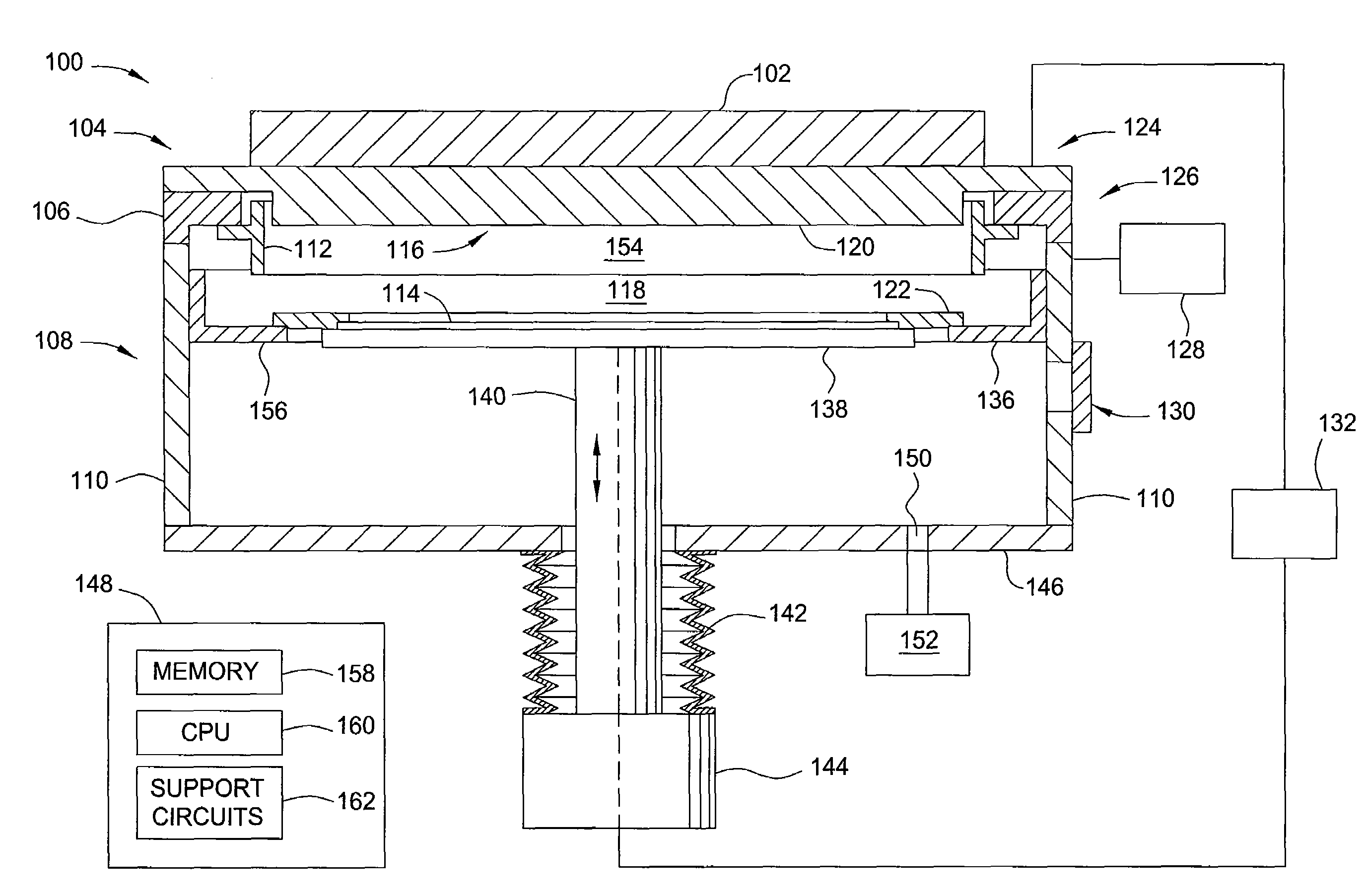
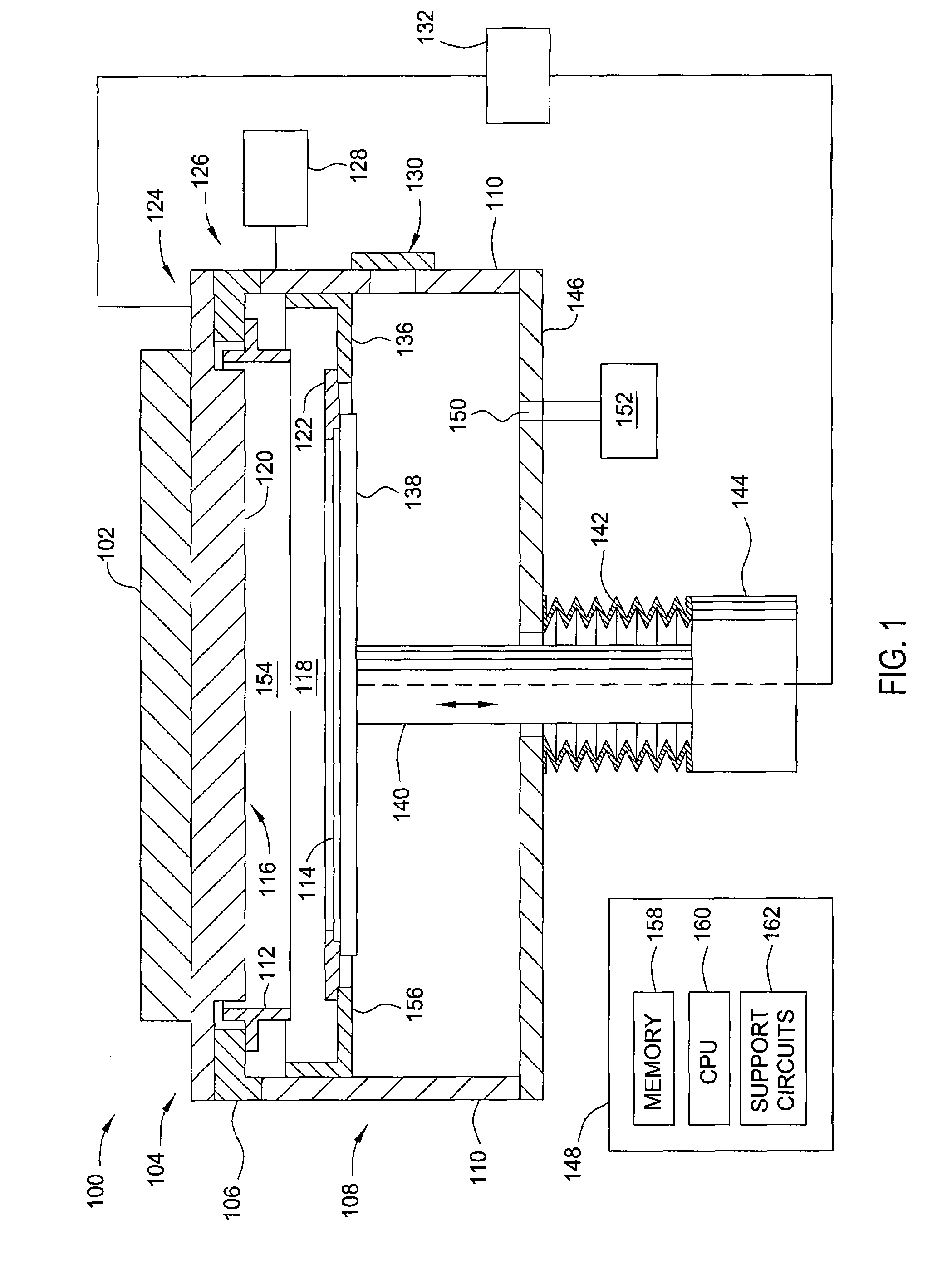
[0019]FIG. 1 illustrates an exemplary reactive sputter process chamber 100 suitable for sputter dep...


PUM

PropertyMeasurementUnit
Temperatureaaaaaaaaaa
Flow rateaaaaaaaaaa

Abstract

Methods for sputter depositing a transparent conductive oxide (TCO) layer are provided in the present invention. The transparent conductive oxide layer may be utilized as a back reflector in a photovoltaic device. In one embodiment, the method includes providing a substrate in a processing chamber, forming a first portion of a transparent conductive oxide layer on the substrate by a first sputter deposition step, and forming a second portion of the transparent conductive oxide layer by a second sputter deposition step.

Description

BACKGROUND OF THE DISCLOSURE[0001]1. Field of the Invention[0002]The present invention relates to methods and apparatus for depositing a transparent conductive film, more specifically, for reactively sputtering depositing a transparent conductive film for photovoltaic devices.[0003]2. Description of the Background Art[0004]Photovoltaic (PV) devices or solar cells are devices which convert sunlight into direct current (DC) electrical power. PV or solar cells typically have one or more p-n junctions. Each junction comprises two different regions within a semiconductor material where one side is denoted as the p-type region and the other as the n-type region. When the p-n junction of the PV cell is exposed to sunlight (consisting of energy from photons), the sunlight is directly converted to electricity through the PV effect. PV solar cells generate a specific amount of electric power and cells are tiled into modules sized to deliver the desired amount of system power. PV modules are c...

Claims


Application Information

Patent Timeline
IPC IPC(8): H01L21/44
CPCC23C14/0073C23C14/086Y02E10/50H01L31/1884H01L31/022466C23C14/34C23C14/08
Inventor LI, YANPINGYE, YANCHAE, YONG-KEEWON, TAE KYUNGKADAM, ANKURSHENG, SHURANLI, LIWEI
Owner APPLIED MATERIALS INC
Why Eureka
Try Eureka