Plasma display panel and method for fabricating the same

Inactive Publication Date: 2008-10-30
LG ELECTRONICS INC
View PDF9 Cites 0 Cited by
  • Summary
  • Abstract
  • Description
  • Claims
  • Application Information

AI Technical Summary

Benefits of technology

[0011]An object of the present invention is to provide a plasma display panel and a method for fabricating the same, in which the amount of wall charges accumulated on a surface of a dielectric layer is controlled without change of a dielectric ratio of the dielectric layer provided in an upper panel of the plasma display panel

Problems solved by technology

However, a current cathode ray tube (CRT) has a limitation in configuring a large screen of 40 inch or greater.
For this reason, since sustain current a

Method used


Image

  • Plasma display panel and method for fabricating the same
  • Plasma display panel and method for fabricating the same
  • Plasma display panel and method for fabricating the same

Examples


Example

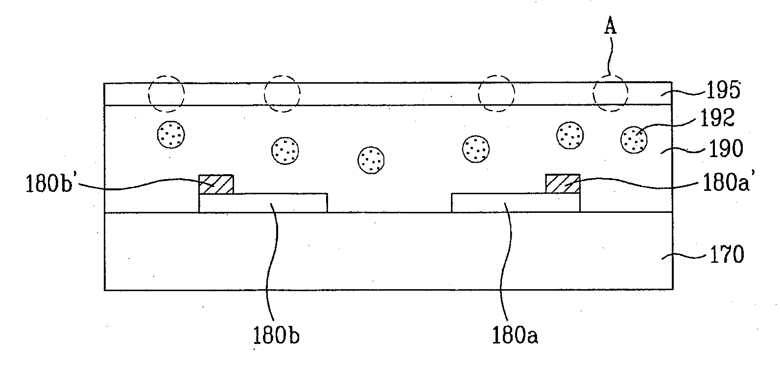
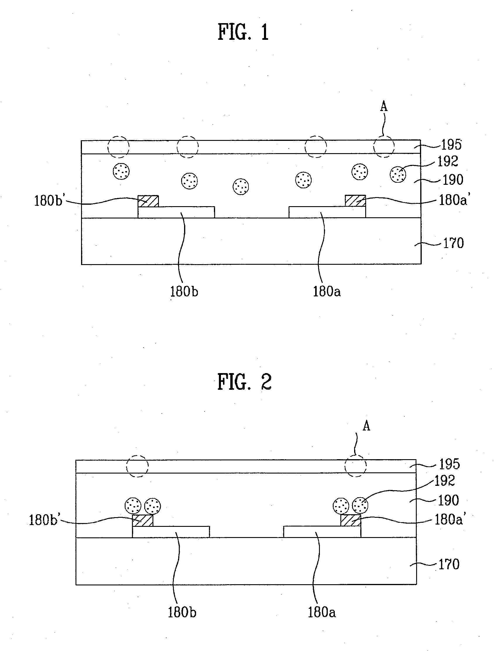
[0041]Although the second embodiment is basically the same as the aforementioned first embodiment, the high dielectric particles 192 are concentrated on the bus electrodes 180a′ and 180b′ in the second embodiment. Unlike the second embodiment, the high dielectric particles 192 are uniformly distributed within the dielectric layer 190 in the first embodiment. The size and composition of the high dielectric particles according to the second embodiment are the same as those of the high dielectric particles according to the first embodiment.

[0042]In the plasma display panel according to the second embodiment of the present invention, capacitance locally increases due to high dielectric particles provided inside the dielectric layer of the front panel during discharge. Accordingly, charged particles are locally accumulated in the dielectric layer where the high dielectric particles are located. For this reason, the amount of local wall charges increases so as to obtain stable discharge c...

Example

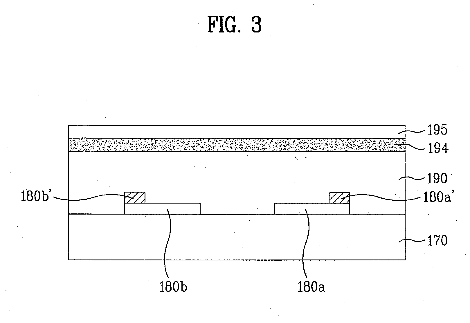
[0045]Although the third embodiment is basically the same as the aforementioned first embodiment, high dielectric particles constitute one layer 194. In other words, as shown, the high dielectric particle layer 194 is formed as a separate layer on the dielectric layer 190. The high dielectric particle layer 194 has a thickness of 1 micrometer to 16 micrometer. Although the dielectric layer 190 conventionally has a thickness of 30 to 40 micrometer, it will have a thin thickness equivalent to the thickness of the high dielectric particle layer 194. Also, although the high dielectric particle layer 194 is provided between the protective layer 195 and the dielectric layer 190 as shown, the high dielectric particle layer 194 may be formed to abut the sustain electrode pairs.

[0046]FIG. 4 illustrates a plasma display panel according to one embodiment of the present invention.

[0047]As shown in FIG. 4, a front panel of the plasma display panel according to the present invention includes sust...


PUM


Abstract

A plasma display panel is disclosed, which includes a first panel provided with an address electrode, a first dielectric, and a phosphor on a first substrate, and a second panel bonded to the first panel by interposing a barrier therebetween, including a transparent electrode, a bus electrode, a second dielectric provided with high dielectric particles, and a protective layer on a second substrate.

Description

[0001]This application claims the benefit of the Korean Patent Application No. 10-2007-0040245, filed on Apr. 25, 2007, which is hereby incorporated by reference as if fully set forth herein.BACKGROUND OF THE INVENTION[0002]1. Field of the Invention[0003]The present invention relates to a plasma display panel, and more particularly, to an upper dielectric layer of a plasma display panel and a method for fabricating the same.[0004]2. Discussion of the Related Art[0005]With the advent of the multimedia age, a display device, which is finer and larger and can display a more natural color, is being required. However, a current cathode ray tube (CRT) has a limitation in configuring a large screen of 40 inch or greater. In this respect, display devices such as a liquid crystal display, a plasma display panel, and a projection television (TV) have been rapidly developed for enlargement to the video field of high picture quality in their use.[0006]The display devices such as the aforementio...

Claims


Application Information

Patent Timeline
IPC IPC(8): H01J1/62H01J9/38
CPCH01J11/12H01J11/40H01J11/38
Inventor LEE, YOUNG HANCHOI, HO SEONGCHOI, SUNG CHUN
Owner LG ELECTRONICS INC
Why Eureka
Try Eureka