Semiconductor circuit

Active Publication Date: 2008-10-30
RENESAS ELECTRONICS CORP
View PDF6 Cites 0 Cited by
  • Summary
  • Abstract
  • Description
  • Claims
  • Application Information

AI Technical Summary

Benefits of technology

[0019]According to the amplifier of the present invention, by connecting the gate of the transistor driving the output and a connecting point forming mirror configuration without using the feedback transistor, it is possible to give feedback corresponding to the common-mode input voltage an

Problems solved by technology

However, since the cascode-connected transistor of the dummy that is prepared separately from the output current path is provided, extra current is needed, and high-speed performance and reduced power consumption cannot be realiz

Method used


Image

  • Semiconductor circuit
  • Semiconductor circuit
  • Semiconductor circuit

Examples


Embodiment Construction

[0036]The invention will now be described herein with reference to illustrative embodiments. Those skilled in the art will recognize that many alternative embodiments can be accomplished using the teachings of the present invention and that the invention is not limited to the embodiments illustrated for explanatory purposes.

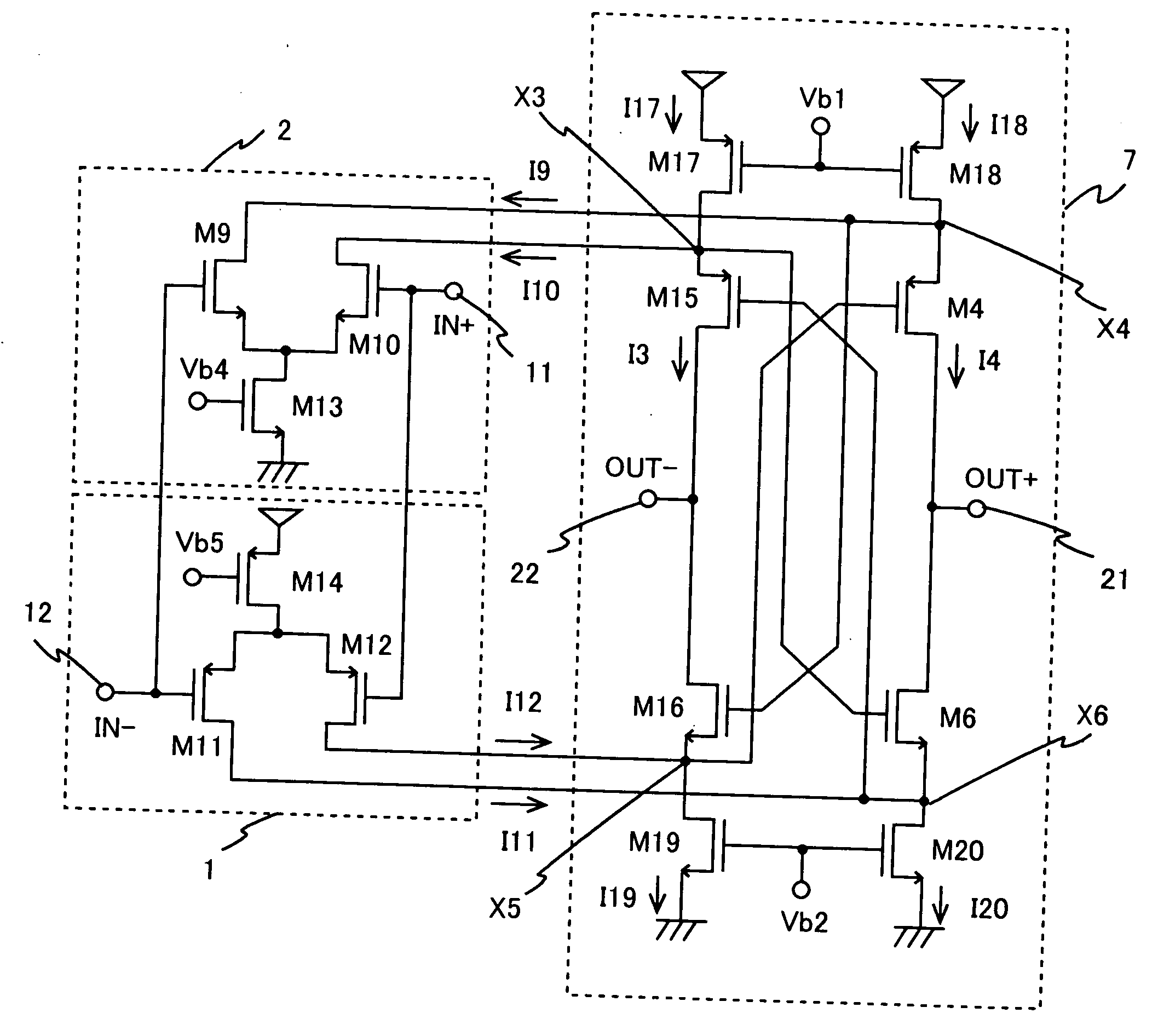
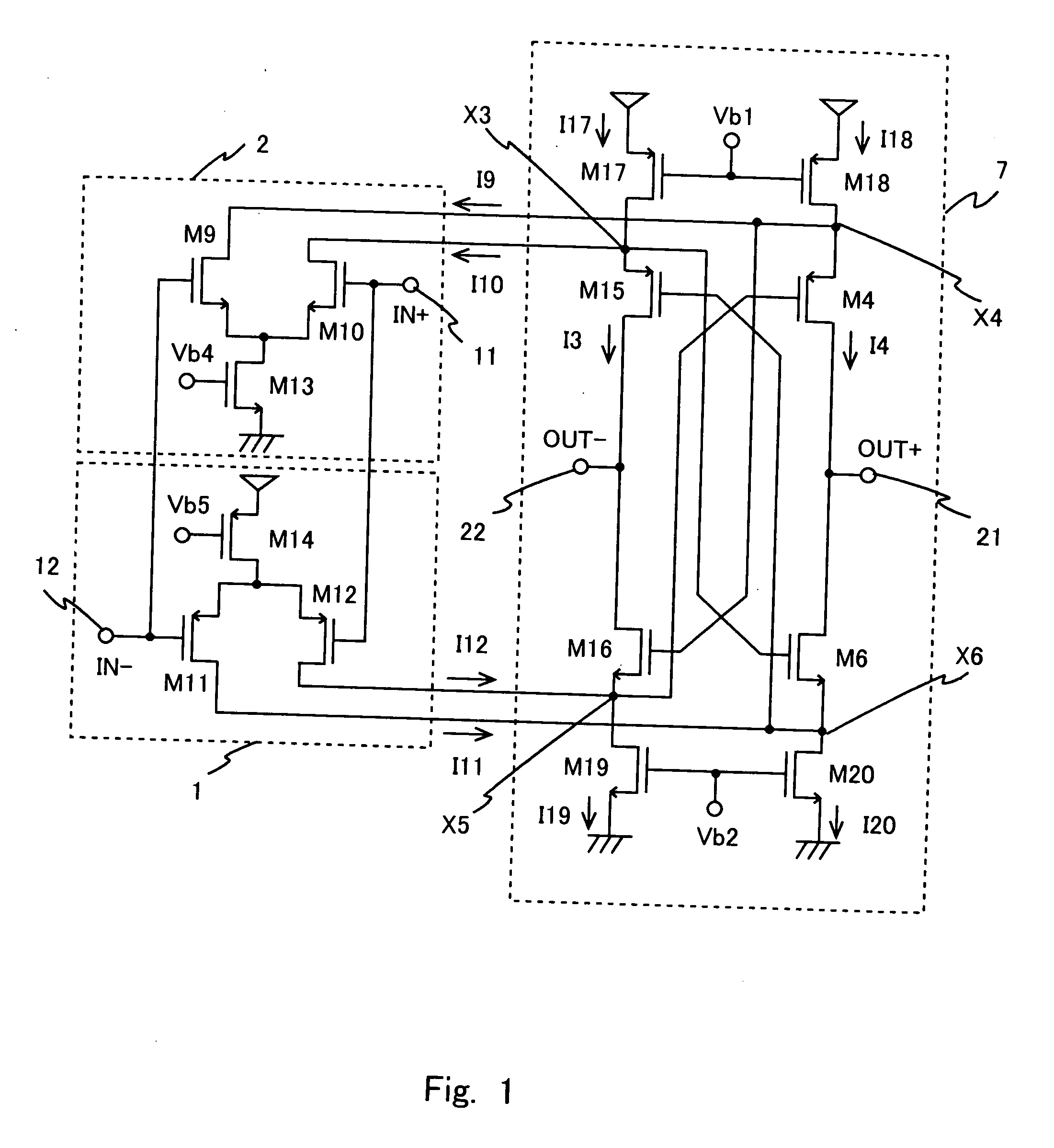
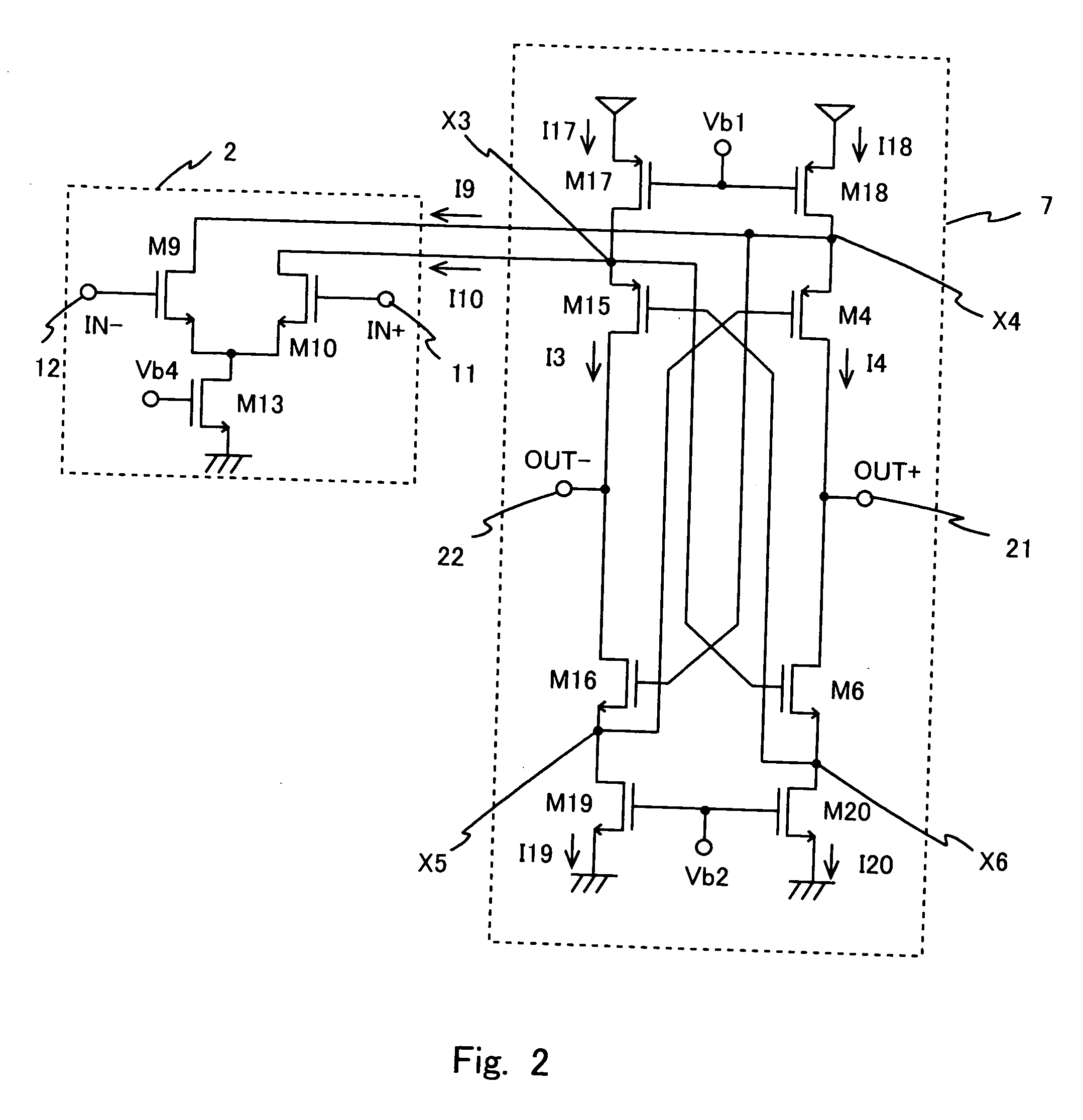
[0037]Hereinafter, the specific embodiment to which the present invention is applied will be described in detail with reference to the drawings. FIG. 1 shows an example of a configuration of a differential output amplifier according to the present embodiment.

[0038]A differential output amplifier 100 includes an input terminal 11 (input IN+), an input terminal 12 (input IN−), and a Pch input part 1 and an Nch input part 2 with respect to wide range common-mode input, an output part 7, an output terminal 21 (output OUT+), and an output terminal 22 (output OUT−).

[0039]The Pch input part 1 includes Pch MOS transistors M11, M12, and M14. The MOS transistor M11 has a g...


PUM


Abstract

An amplifier includes differential output and input stages. The differential output stage includes first and second current paths outputting differential signals and connected between first and second power supplies. The first current path includes a first resistance between the first power supply and a first node, first and second transistors between the first node and a second node, and a second resistance between the second node and the second power supply. The second current path includes a third resistance between the first power supply and a third node, third and fourth transistors between the third node and a fourth node, and a fourth resistance between the fourth node and the second power supply. Each gate of the first to fourth transistors is connected to each of the fourth to first nodes, respectively, and output current of the differential input stage is connected to the first and third nodes.

Description

BACKGROUND OF THE INVENTION[0001]1. Field of the Invention[0002]The present invention relates to a differential amplifier. More specifically, the present invention relates to a differential amplifier stabilizing differential output by controlling output impedance.[0003]2. Description of Related Art[0004]FIG. 9 shows a differential operational amplifier configuring an input stage by NMOS-type differential pair and PMOS-type differential pair and an output stage by cascode current mirror as an amplifier including a typical wide-range common-mode input.[0005]A typical Pch input part 1 and Nch input part 2 with respect to a wide-range common-mode input are configured by input terminals IN+ and IN−, Pch MOS transistors M11, M12, M14, and Nch MOS transistors M9, M10, M13. The MOS transistors M13 and M14 are set to constant current sources by potential of Vb4 and Vb5 that are gate potential.[0006]An output part 3 driving output terminal OUT is configured by cascode-connected Pch MOS transi...

Claims


Application Information

Patent Timeline
IPC IPC(8): H03F3/45
CPCH03F3/3022H03F3/45219H03F2203/30015H03F2203/45318H03F2203/45626
Inventor SUZUKI, YASUFUMI
Owner RENESAS ELECTRONICS CORP
Why Eureka
Try Eureka