
Sub-pixel current measurement for OLED display

a technology of oled display and subpixel current, which is applied in the direction of instruments, static indicating devices, etc., can solve the problems of low accuracy of subpixel current measurement, limited number of lines, and low accuracy of pm oled display, so as to facilitate accurate measurement of subpixel current and relatively large subpixel current

Inactive Publication Date: 2008-10-30
LEADIS TECH
View PDF17 Cites 32 Cited by
  • Summary
  • Abstract
  • Description
  • Claims
  • Application Information

AI Technical Summary

Benefits of technology

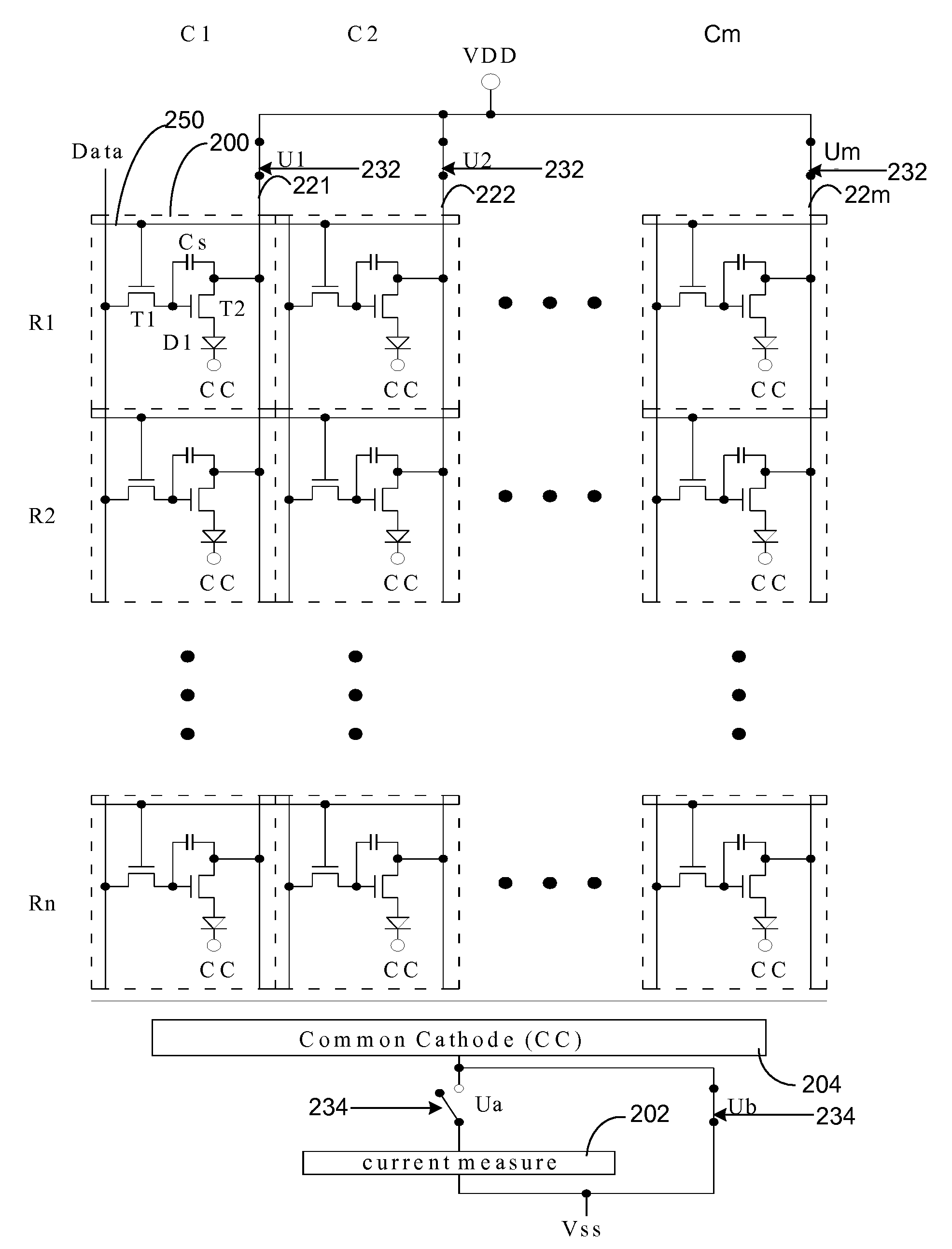
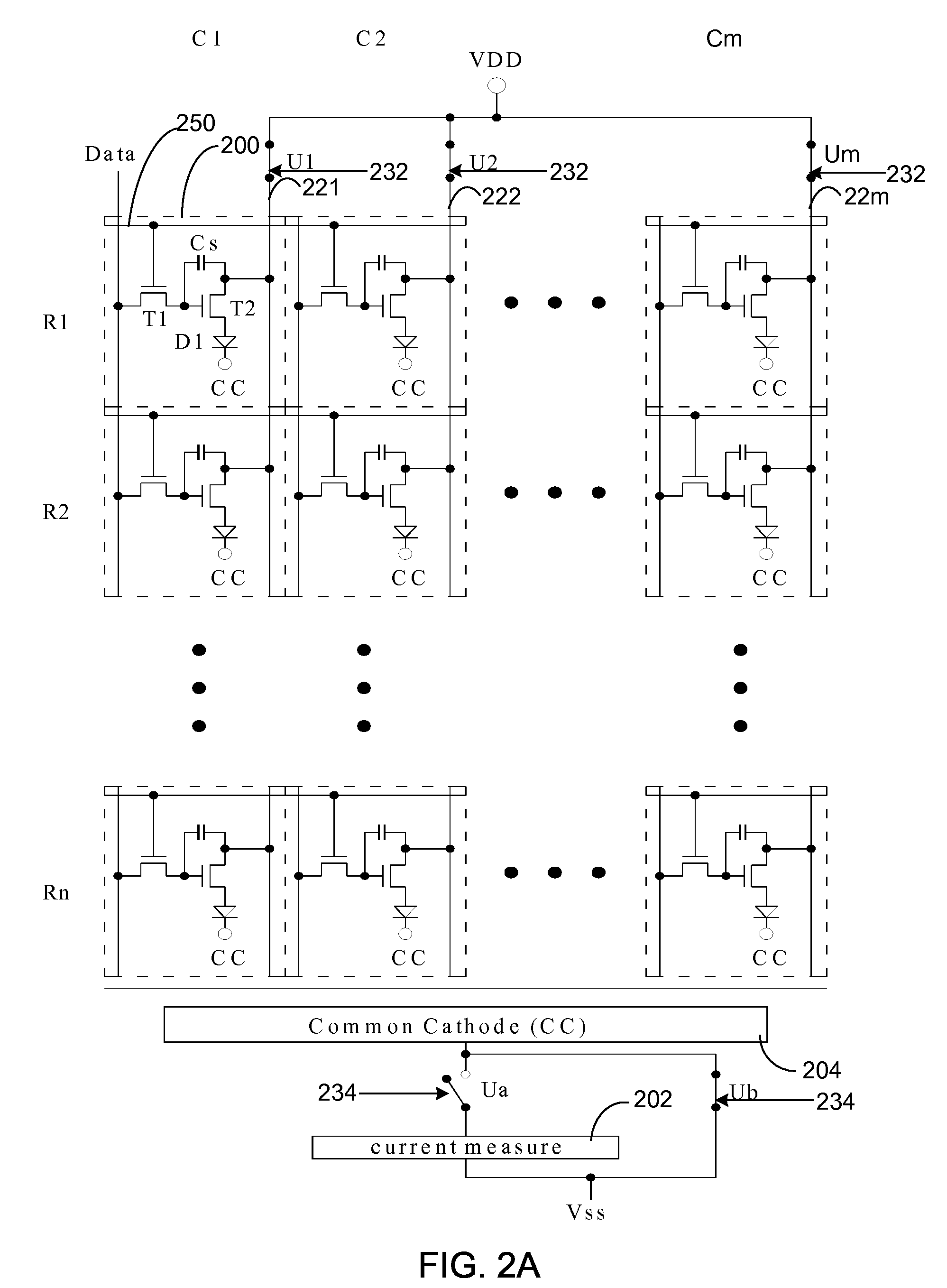
[0015]Embodiments of the present invention include an active matrix drive system for driving an emissive display device and configured to measure sub-pixel current in the emissive display device, where one or more power column power lines of the emissive display device are disconnected from the supply voltage while sub-pixel current is measured. As a result, the sub-pixel current is relatively large compared to the background current of the emissive display device, which facilitates accurate measurement of the sub-pixel current.

Problems solved by technology

While PM OLEDs are fairly simple structures to design and fabricate, they demand relatively expensive, current-sourced drive electronics to operate effectively and are limited to the number of lines because only one line can be on at a time and therefore the PM OLED must have overall brightness equal to the desired average brightness times the number of lines.
Thus, PM OLED displays are typically limited to under 100 lines.
In addition, their power consumption is significantly higher than that required by an active-matrix OLED.
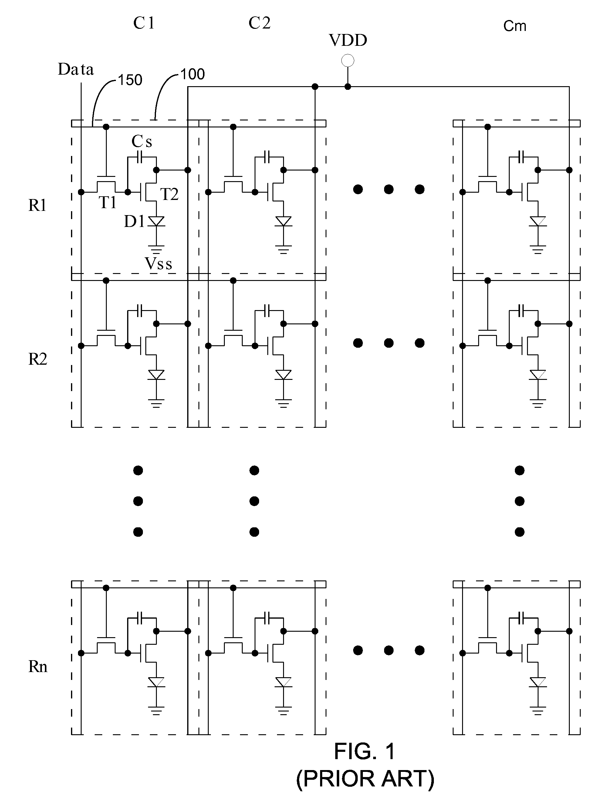
However, uniform TFTs are very difficult to produce and thus the current supplied by TFTs T2 in conventional OLED displays is often non-uniform, resulting in non-uniform display brightness.
However, accurately measuring the actual current through each OLED of the subpixels of the OLED panel is not simple, due to the large number of pixels in an OLED display panel.
Since the background current (10 microamperes) is very large compared to the current increase resulting from a single turned-on sub-pixel (between a few nanoamperes and one microampere), it is extremely difficult to measure the sub-pixel current accurately.

Method used


Image

  • Sub-pixel current measurement for OLED display
  • Sub-pixel current measurement for OLED display
  • Sub-pixel current measurement for OLED display

Examples


Embodiment Construction

[0024]The Figures (FIG.) and the following description relate to preferred embodiments of the present invention by way of illustration only. It should be noted that from the following discussion, alternative embodiments of the structures and methods disclosed herein will be readily recognized as viable alternatives that may be employed without departing from the principles of the claimed invention.

[0025]Reference will now be made in detail to several embodiments of the present invention(s), examples of which are illustrated in the accompanying figures. It is noted that wherever practicable similar or like reference numbers may be used in the figures and may indicate similar or like functionality. The figures depict embodiments of the present invention for purposes of illustration only. One skilled in the art will readily recognize from the following description that alternative embodiments of the structures and methods illustrated herein may be employed without departing from the pr...


PUM


Abstract

An active matrix drive system drives an emissive display device such as an organic light-emitting diode display and is configured to measure sub-pixel current in the emissive display device. One or more power column power lines of the emissive display device are turned off while sub-pixel current is measured. As a result, the sub-pixel current is relative large compared to the background current of the emissive display device, which facilitates accurate measurement of the sub-pixel current.

Description

CROSS-REFERENCE TO RELATED APPLICATION[0001]This application claims priority under 35 U.S.C. § 119(e) from co-pending U.S. Provisional Patent Application No. 60 / 925,990 entitled “Sub-pixel Current Measurement” filed on Apr. 24, 2007, which is incorporated by reference herein in its entirety.BACKGROUND OF THE INVENTION[0002]1. Field of the Invention[0003]The present invention relates to measuring the sub-pixel current of an emissive display such as an OLED (Organic Light-Emitting Diode) display.[0004]2. Description of the Related Arts[0005]An OLED display is generally comprised of an array of organic light emitting diodes (OLEDs) that have carbon-based films disposed between two charged electrodes. Generally one electrode is comprised of a transparent conductor, for example, indium tin oxide (ITO). Generally, the organic material films are comprised of a hole-injection layer, a hole-transport layer, an emissive layer and an electron-transport layer. When voltage is applied to the OLE...

Claims


Application Information

Patent Timeline
Patent Type & Authority Applications(United States)
IPC IPC(8): G09G3/30
CPCG09G3/3225G09G3/3233G09G2320/0233G09G2320/029G09G2320/0295G09G2330/02
Inventor NAUGLER, WALTER EDWARDKANG, SUNG GUKIM, CHEON HONG
Owner LEADIS TECH
Learn More