Method of blocking a void during contact formation process and device having the same

a technology of contact formation and blocking void, which is applied in the direction of semiconductor devices, semiconductor/solid-state device details, electrical apparatus, etc., can solve the problem of negative affecting the resistivity of the source/drain region

Inactive Publication Date: 2008-11-06
NXP USA INC
View PDF4 Cites 202 Cited by
  • Summary
  • Abstract
  • Description
  • Claims
  • Application Information

AI Technical Summary

Problems solved by technology

However, exposing the source / drain region more than once during a contact opening formation sequence can negatively affect the resistivity of the source / drain region.

Method used


Image

  • Method of blocking a void during contact formation process and device having the same
  • Method of blocking a void during contact formation process and device having the same
  • Method of blocking a void during contact formation process and device having the same

Examples


Embodiment Construction

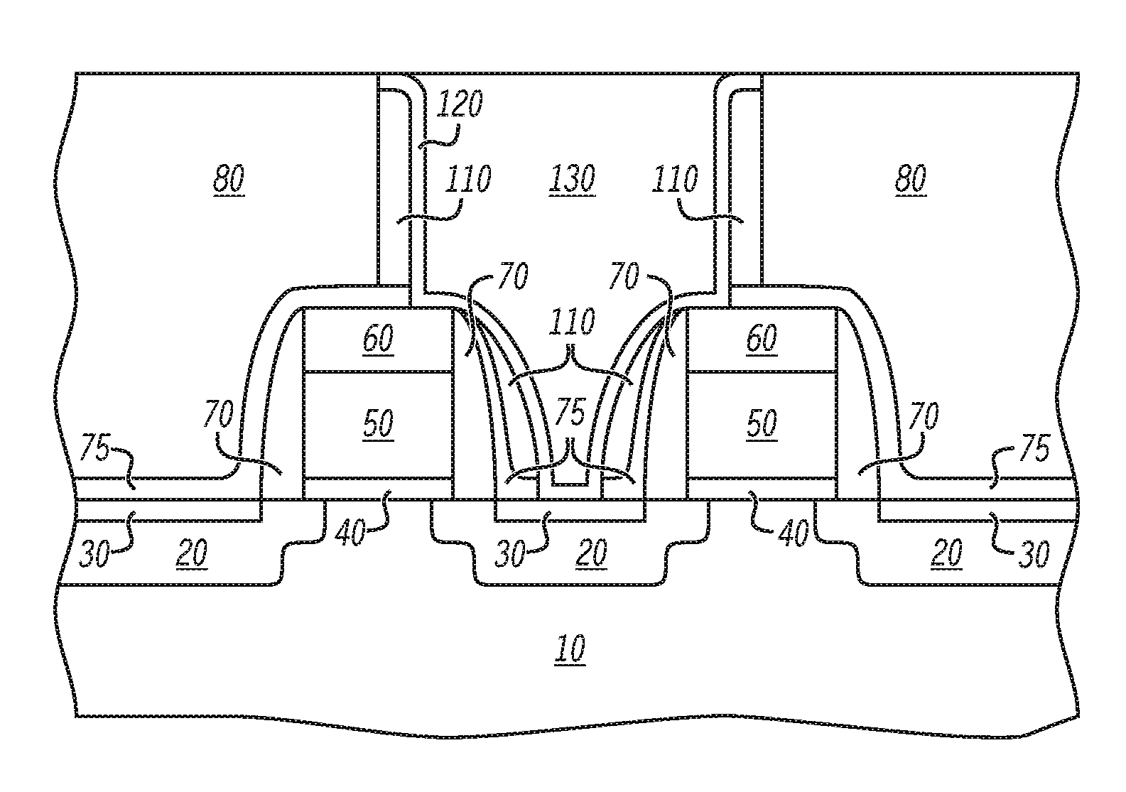
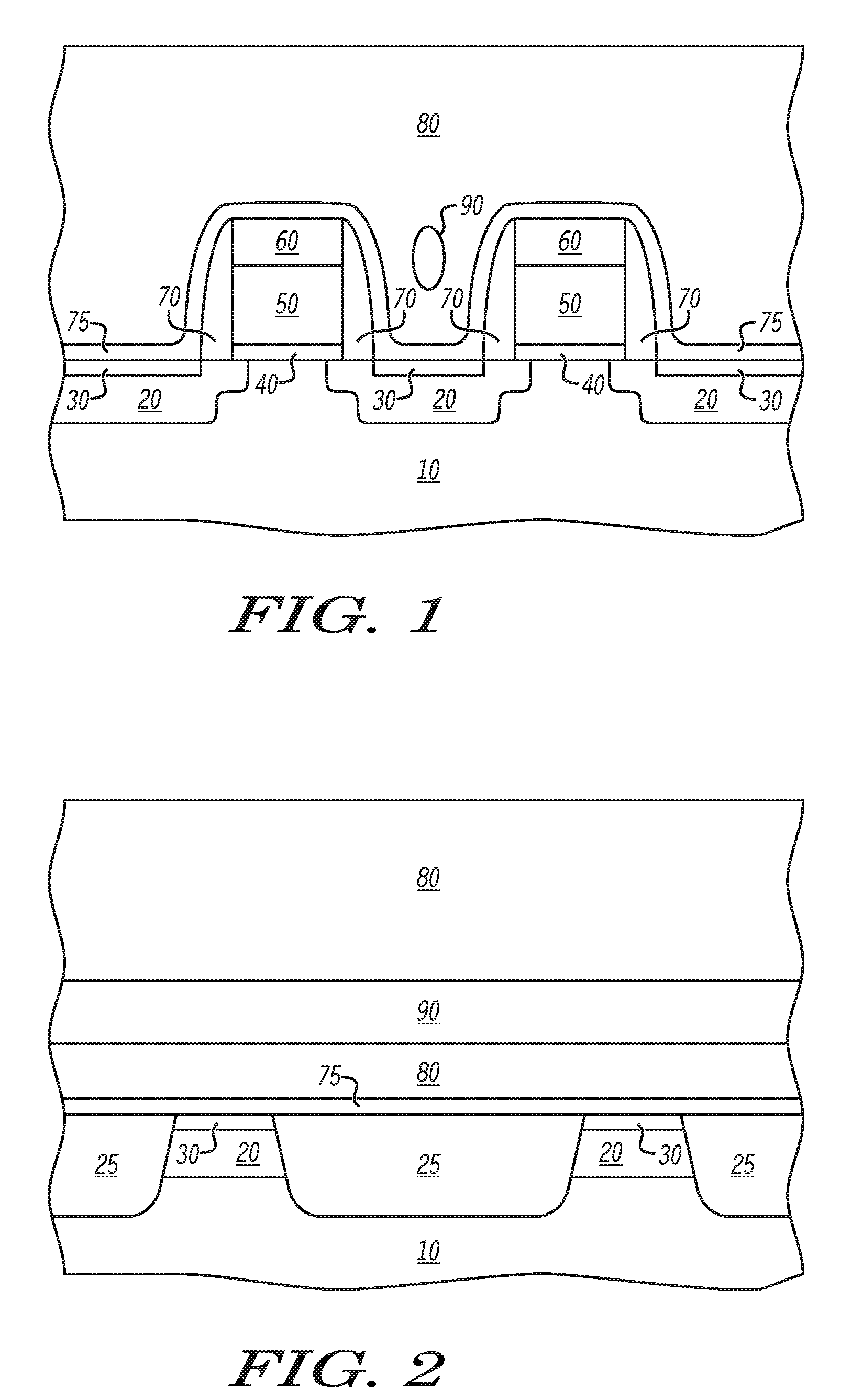
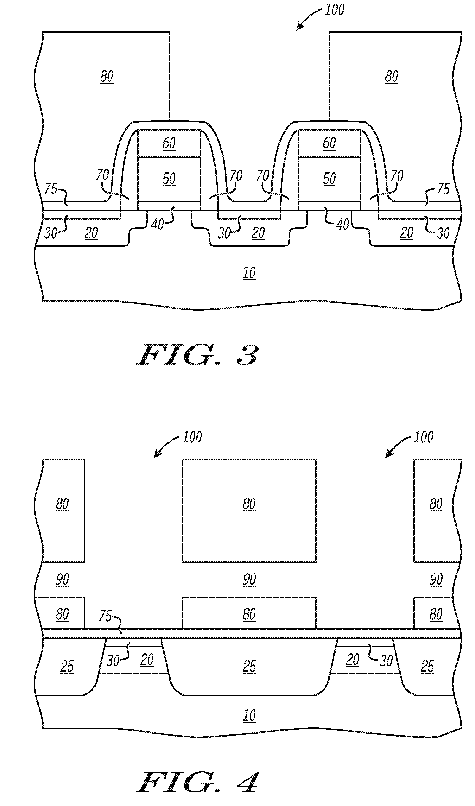
[0014]An electronic device can include different conductive regions. The electronic device can also include an insulating layer including a void extending between different portions of the insulating layer. A section of one opening through a portion of the insulating layer and another section of another opening through the other portion of the insulating layer can intersect the void. A liner layer can lie within the sections of the openings and substantially block the void.

[0015]In one aspect, a stressor layer can be deposited over the conductive regions prior to forming the insulating layer, and the liner layer can be formed over the stressor layer within the openings. In another aspect, a silicide layer can be formed over the conductive regions, and an etch-stop layer can be formed over the silicide layer prior to forming the insulating layer. The liner layer can be formed within one opening, the other opening, or any combination thereof, and a portion of the etch-stop layer can b...


PUM


Abstract

An electronic device can include conductive regions. A void can extend between different portions of an insulating layer. Different openings can intersect the void. A liner layer can substantially block the void, substantially preventing subsequently forming an electrical leakage path along the void. In one aspect, a stressor layer can be deposited over the conductive regions prior to forming the insulating layer. The liner layer can be formed over the stressor layer within the different openings through the insulating layer. In another aspect, an etch-stop layer can be formed over a silicide layer prior to forming the insulating layer. After removing a portion of the liner layer, a portion of the etch-stop layer can be removed to expose the silicide layer within the different openings. In yet another aspect, a nitride layer can lie between a substrate and the insulating layer and include a section of the openings.

Description

BACKGROUND[0001]1. Field of the Disclosure[0002]This disclosure pertains, in general, to semiconductor processing and, more specifically, to forming an integrated circuit device with contact openings.[0003]2. Description of the Related Art[0004]Interconnect technology is a factor in the ability to reduce the area of integrated circuit devices. Multi-level metallization layouts have assisted dimension shrinkage by having multiple metal lines share the same area of the device. In a multi-level metallization layout, a dielectric layer, termed an interlevel dielectric layer (“ILD”) or a pre-metal dielectric (“PMD”) layer, is formed between the first metal layer and the transistors. Typically, the dielectric layer is formed to isolate the metal layer from the transistors. To electrically connect the underlying gates of the transistors or the substrate (i.e. the source or drain region) to the first metal line, a contact opening is etched through the ILD layer and filled with a conductive ...

Claims


Application Information

Patent Timeline
Patent Type & Authority Applications(United States)
IPC IPC(8): H01L23/528H01L21/4763
CPCH01L21/7682H01L21/76831H01L21/76897H01L23/485H01L2924/0002H01L2924/00
Inventor TSANG, YUK L.
Owner NXP USA INC
Why Eureka
Try Eureka