Non-volatile semiconductor memory device and method of making the same

a non-volatile, memory device technology, applied in semiconductor devices, digital storage, instruments, etc., can solve the problems of difficult to provide a larger capacity by a smaller design rule, difficult to fabricate fine patterns such as word-lines and wirings, and increase the cost of three-dimensional structures

Inactive Publication Date: 2010-02-18
KK TOSHIBA
View PDF5 Cites 52 Cited by
  • Summary
  • Abstract
  • Description
  • Claims
  • Application Information

AI Technical Summary

Problems solved by technology

With general manufacturing methods, it becomes harder to fabricate fine patterns such as word-lines and wirings, making it harder to provide a larger capacity by a smaller design rule.
This inevitably causes a cost increase due to the three-dimensional structure.

Method used


Image

  • Non-volatile semiconductor memory device and method of making the same
  • Non-volatile semiconductor memory device and method of making the same
  • Non-volatile semiconductor memory device and method of making the same

Examples


first embodiment

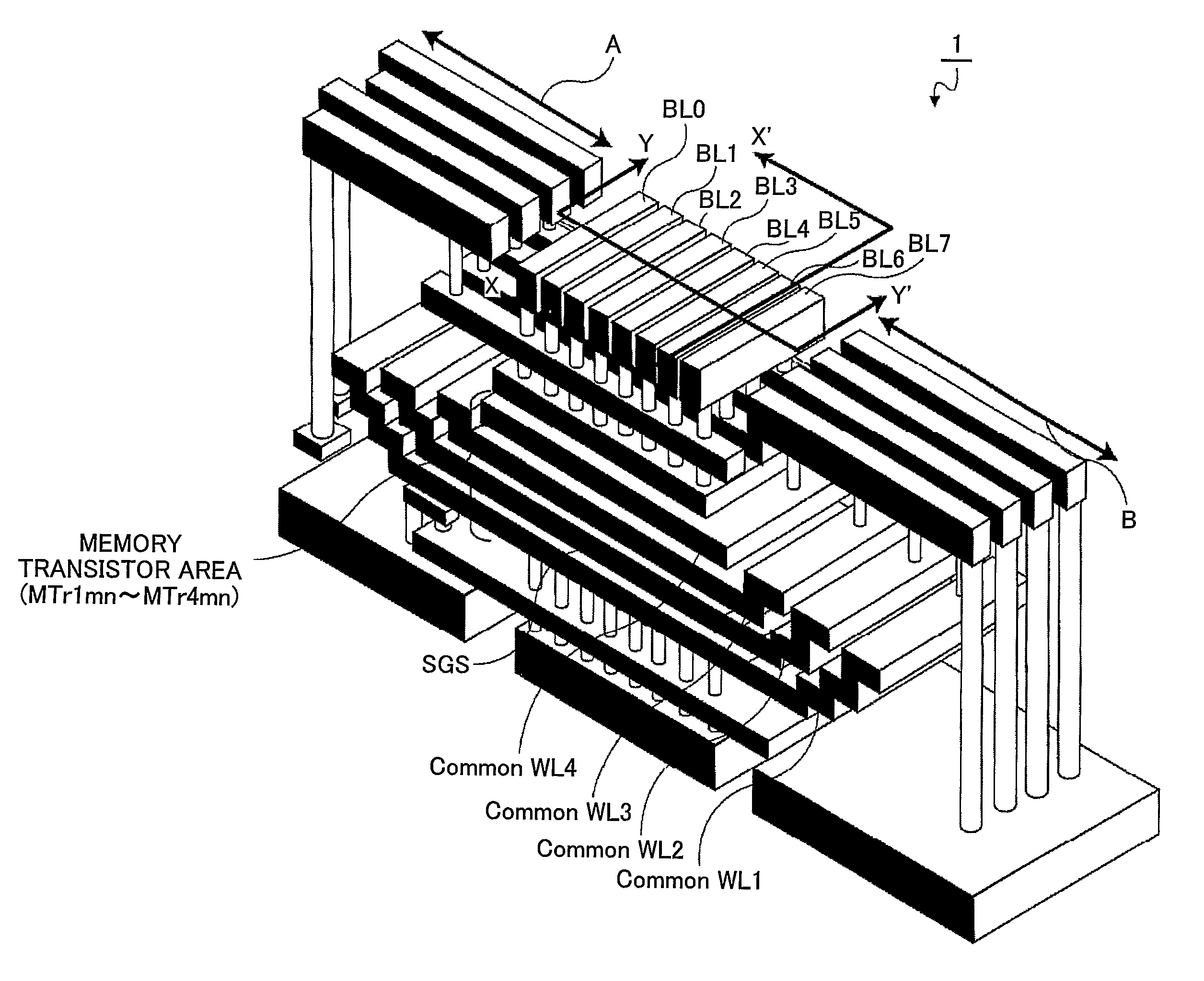
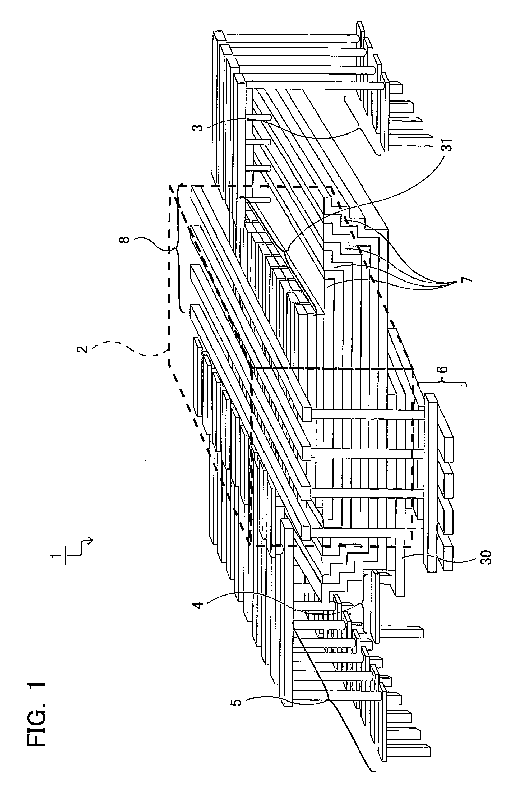
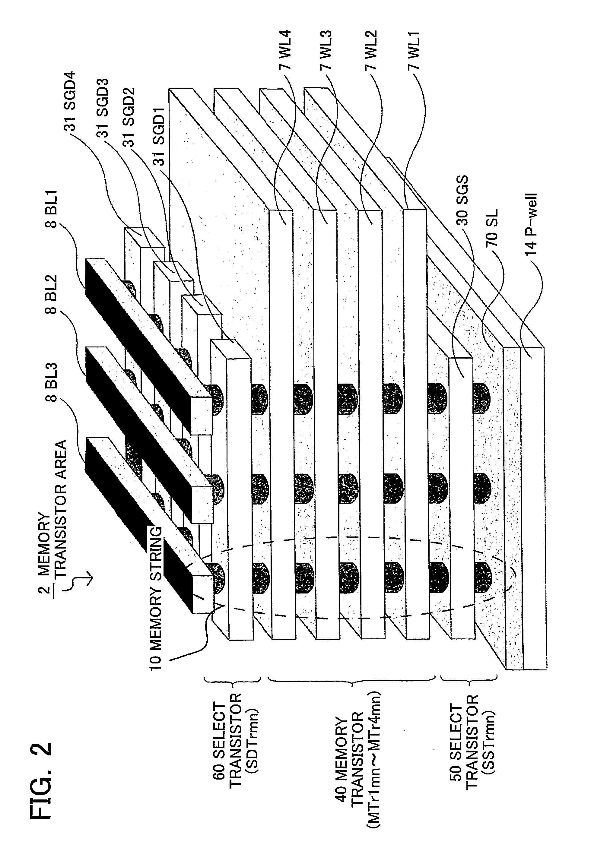
[0041]FIG. 1 shows a schematic configuration diagram of a non-volatile semiconductor memory device 1 according to a first embodiment of the present invention. The non-volatile semiconductor memory device 1 according to the first embodiment of the present invention includes components such as a memory transistor area 2, a word-line driver circuit 3, a source select gate line (SGS) driver circuit 4, a drain select gate line (SGD) driver circuit 5, a sense amplifier 6, a word-line WL (7), a bit-line BL 8, a source select gate line SGS 30, and a drain select gate line SGD 31. With reference to FIG. 1, in the non-volatile semiconductor memory device 1 according to the first embodiment of the present invention, the memory transistor area 2 includes a plurality of memory transistors. The memory transistors are collectively formed by depositing a plurality of laminated semiconductor layers. Also with reference to FIG. 1, the word-line WL (7) in each semiconductor layer extends in the memory...


PUM


Abstract

A non-volatile semiconductor memory device according to the present invention includes a substrate; a first word-line provided above the substrate surface, the first word-line having a plate shape in an area where a memory cell is formed; a second word-line provided above the first word-line surface, the second word-line having a plate shape; a plurality of metal wirings connecting the first and second word-lines with a driver circuit; and a plurality of contacts connecting the first and second word-lines with the metal wirings. The contact of the first word-line is formed in a first word-line contact area. The contact of the second word-line is formed in a second word-line contact area. The first word-line contact area is provided on a surface of the first word-line that is drawn to the second word-line contact area.

Description

FIELD OF THE INVENTION[0001]The present invention relates to semiconductor memory devices that are capable of electrically rewriting data, and more particularly, to non-volatile semiconductor memory devices.DESCRIPTION OF THE RELATED ART[0002]Compact and large-capacity non-volatile semiconductor memory devices have been increasingly required. NAND flash memories draw attention to the possibility of higher integration and a larger capacity. With general manufacturing methods, it becomes harder to fabricate fine patterns such as word-lines and wirings, making it harder to provide a larger capacity by a smaller design rule.[0003]For the purpose of more highly integrated memory devices, a large number of semiconductor memory devices have recently been proposed that include three-dimensionally disposed memory cells (see, for example, JP 2003-078044, U.S. Pat. No. 5,599,724, U.S. Pat. No. 5,707,885, and Endoh et al., “Novel Ultrahigh-Density Flash Memory With a Stacked-Surrounding Gate Tr...

Claims


Application Information

Patent Timeline
Patent Type & Authority Applications(United States)
IPC IPC(8): G11C16/06H01L29/792H01L21/4763
CPCG11C16/0483H01L21/8221H01L27/0688H01L27/11582H01L27/11568H01L27/11578H01L27/105H10B43/50H10B43/20H10B43/30H10B43/27H01L21/76877
Inventor KIDOH, MASARUTANAKA, HIROYASUKITO, MASARUKATSUMATA, RYOTAAOCHI, HIDEAKISATO, MITSURU
Owner KK TOSHIBA
Why Eureka
Try Eureka