Low Resistance Source Drain Contact Formation

a technology of low resistance and drain contact, applied in the direction of basic electric elements, electrical equipment, semiconductor devices, etc., can solve the problem that boron is not an ideal dopant for ge-based transistors, and achieve the effect of reducing contact resistan

Active Publication Date: 2017-07-27
IBM CORP +1
View PDF0 Cites 51 Cited by
  • Summary
  • Abstract
  • Description
  • Claims
  • Application Information

AI Technical Summary

Benefits of technology

[0005]The present invention provides techniques for forming gallium (Ga)-doped source drain contacts in Ge-based transistors using a rapid anneal to increase amounts of Ga above chemical stability concentrations and thereby greatly reduce contact resistance. In one aspect of the invention, a method for forming Ga-doped p-type source and drain contacts is provided. The method includes the steps of: forming a transistor comprising source and drain regions interconnected by a channel region and at least one gate configured to regulate current flow through the channel region; depositing a dielectric over the transistor; forming contact trenches in the dielectric over, and extending down to, the source and drain regions; depositing an epitaxial material into the contact trenches; implanting gallium ions into the epitaxial material to form an amorphous gallium-doped layer; and annealing the amorphous gallium-doped layer under conditions sufficient to form a crystalline gallium-doped layer having a homogenous gallium concentration of greater than about 5×10²⁰ atoms per cubic centimeter (at. / cm3).

Problems solved by technology

Thus, boron is not an ideal dopant for Ge-based transistors.

Method used


Image

  • Low Resistance Source Drain Contact Formation
  • Low Resistance Source Drain Contact Formation
  • Low Resistance Source Drain Contact Formation

Examples


Embodiment Construction

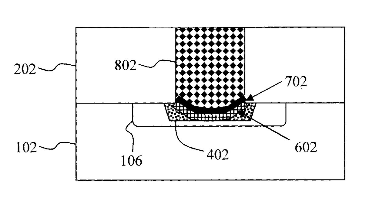
[0023]Provided herein are techniques for forming Ga-doped p-type source and drain contacts. The present techniques may be used in conjunction with those described in U.S. patent application Ser. No. ______, entitled “Low Resistance Source Drain Contact Formation With Trench Metastable Alloys and Laser Annealing,” designated as Attorney Docket Number YOR920160026US1, the contents of which are incorporated by reference as if fully set forth herein.

[0024]As compared to conventional p-type dopants such as boron (see above), Ga has a high solubility in Ge. For instance, the solubility of Ga in pure Ge is about 5.0'1020 atoms per cubic centimeter (at. / cm3) in pure Ge. See, for example, C. Claeys et al., “Germanium-Based Technologies: From Materials to Devices,” Elsevier, New York p. 338 (2007), the contents of which are incorporated by reference as if fully set forth herein.

[0025]Advantageously, by way of a rapid re-crystallization annealing process, the present techniques may be employed...


PUM


Abstract

Techniques for forming Ga-doped source drain contacts in Ge-based transistors are provided. In one aspect, a method for forming Ga-doped source and drain contacts includes the steps of: depositing a dielectric over a transistor; depositing a dielectric over the transistor; forming contact trenches in the dielectric over, and extending down to, source and drain regions of the transistor; depositing an epitaxial material into the contact trenches; implanting gallium ions into the epitaxial material to form an amorphous gallium-doped layer; and annealing the amorphous gallium-doped layer under conditions sufficient to form a crystalline gallium-doped layer having a homogenous gallium concentration of greater than about 5×10²⁰ at./cm3. Transistor devices are also provided utilizing the present Ga-doped source and drain contacts.

Description

FIELD OF THE INVENTION[0001]The present invention relates to low resistance source drain contacts in germanium (Ge)-based transistors, and more particularly, to techniques for forming gallium (Ga)-doped source drain contacts in Ge-based transistors using a rapid anneal to increase amounts of Ga above chemical stability concentrations and thereby greatly reduce contact resistance.BACKGROUND OF THE INVENTION[0002]Transistors typically include at least one gate over a channel region, and source and drain regions on opposite sides of a channel region, and at least one gate that regulates current flow through the channel. Contacts to the source and drain regions are often made by first forming a metal silicide on the base source drain material, then depositing a dielectric over the transistor, patterning contact trenches in the dielectric, and lastly forming metal source drain contacts in the contact trenches.[0003]The contact resistance between the metal contacts and the source drain ma...

Claims


Application Information

Patent Timeline
Patent Type & Authority Applications(United States)
IPC IPC(8): H01L29/08H01L29/167H01L29/417H01L21/324H01L29/78H01L21/265H01L29/45H01L29/66H01L29/165H01L29/161H01L21/02
CPCH01L29/0847H01L29/161H01L29/167H01L29/41725H01L21/324H01L21/02057H01L29/7848H01L21/02532H01L21/02592H01L29/45H01L29/665H01L29/165H01L21/26513H01L21/28518H01L21/823814H01L29/66545H01L29/66636
Inventor GLUSCHENKOV, OLEGLIU, ZUOGUANGMOCHIZUKI, SHOGONIIMI, HIROAKIYEH, CHUN-CHEN
Owner IBM CORP
Why Eureka
Try Eureka