

High-density phase change cell array and phase change memory device having the same
a phase change memory and cell array technology, applied in semiconductor devices, digital storage, instruments, etc., can solve the problems of unsuitable conventional phase change memory devices adopting cell structures that are unsuitable for high-density phase change memory devices
- Summary
- Abstract
- Description
- Claims
- Application Information
AI Technical Summary
Benefits of technology
Problems solved by technology
Method used
Image

Examples
Embodiment Construction
[0033] Reference now should be made to the drawings, in which the same reference numerals are used throughout the different drawings to designate the same or similar components.
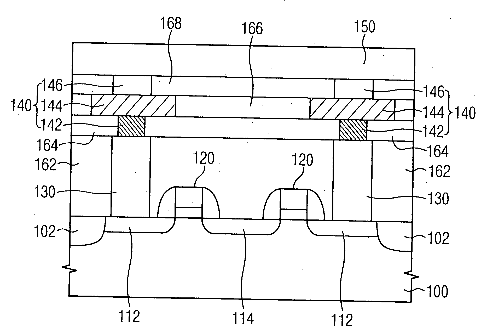
[0034]FIG. 4 is a circuit diagram showing the equivalent circuit of a unit cell that constitutes a phase change memory device according to an embodiment of the present invention. FIG. 5 is a block diagram showing a memory cell array in which the unit cell of FIG. 4 is repeated according to the embodiment of the present invention.
[0035] Referring to FIG. 4, the unit cell includes an access transistor TA and a phase change resistance element GST. The upper electrode of the phase change resistance element GST is connected to a bit line BL. Additionally, the source of the access transistor TA is connected to the lower electrode of the phase change resistance element GST and the drain thereof is connected to a power line. The equivalent circuit of the present invention is different from that of FIG. 2 in that th...
PUM
 Abstract
Description
Claims
Application Information