Method for avoiding oxide undercut during pre-silicide clean for thin spacer FETs

a thin spacer and pre-silicide cleaning technology, applied in semiconductor devices, semiconductor/solid-state device details, electrical apparatus, etc., can solve the problems of dielectric etch stop under the spacer b>25/b> becoming severely undercut at regions

Inactive Publication Date: 2006-01-31
AURIGA INNOVATIONS INC
View PDF7 Cites 51 Cited by
  • Summary
  • Abstract
  • Description
  • Claims
  • Application Information

AI Technical Summary

Benefits of technology

[0008]It is thus an object of the present invention to provide a method for avoiding the dielectric, e.g., oxide, undercut when performing the clean step prior to silicide formation, particularly for thin spacer MOSFETS.
[0009]In accordance with this objective, it has been found that the formation of a thin nitride plug encapsulating and sealing a segment of the dielectric etch stop layer underlying the vertical spacer elements will avoid the aforementioned undercut and associated problems.
[0014]In either variation, the nitride plug effectively seals the portion of the dielectric (oxide) layer underlying the spacer elements to prevent the oxide removal and undercut caused by the pre-silicide cleaning process.

Problems solved by technology

While this dielectric etch stop prevents recessing of the substrate during reactive ion etching (RIE) of the spacer, it has the disadvantage of being susceptible to removal or undercut during the extensive preclean that must be utilized prior to silicide formation.
While this dielectric etch stop prevents recessing of the substrate during spacer RIE, it has the disadvantage of being susceptible to removal or undercut during the extensive pre-clean that must be utilized prior to silicide formation.
However, as illustrated in FIG. 1(d), the problem with this lengthy oxide strip is that the dielectric etch stop beneath the spacers 25 becomes severely undercut at regions 40a, 40b.
These aforementioned problems are particularly acute for transistors with the thin spacer geometries required for (which becoming continued CMOS scaling.

Method used


Image

  • Method for avoiding oxide undercut during pre-silicide clean for thin spacer FETs
  • Method for avoiding oxide undercut during pre-silicide clean for thin spacer FETs
  • Method for avoiding oxide undercut during pre-silicide clean for thin spacer FETs

Examples


Embodiment Construction

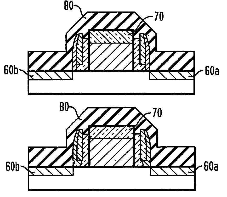
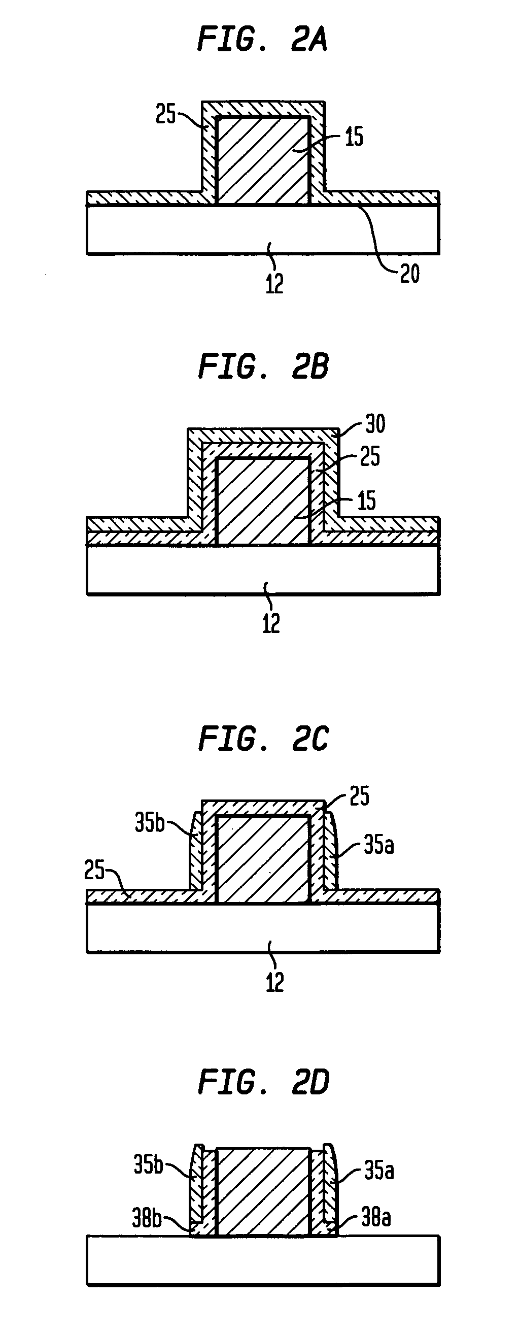
[0022]FIGS. 2(a)–2(h) depict the methodology for avoiding oxide undercut when performing a pre-silicide clean step to remove residual material from the silicon surfaces (either source / drain or gate regions). This methodology enables the formation of transistors with thin spacer geometries for improving FET series resistance.

[0023]The various processing steps and materials used in fabricating the CMOS device of the present invention, together with various embodiments thereof, will now be described in greater detail by the discussion that follows.

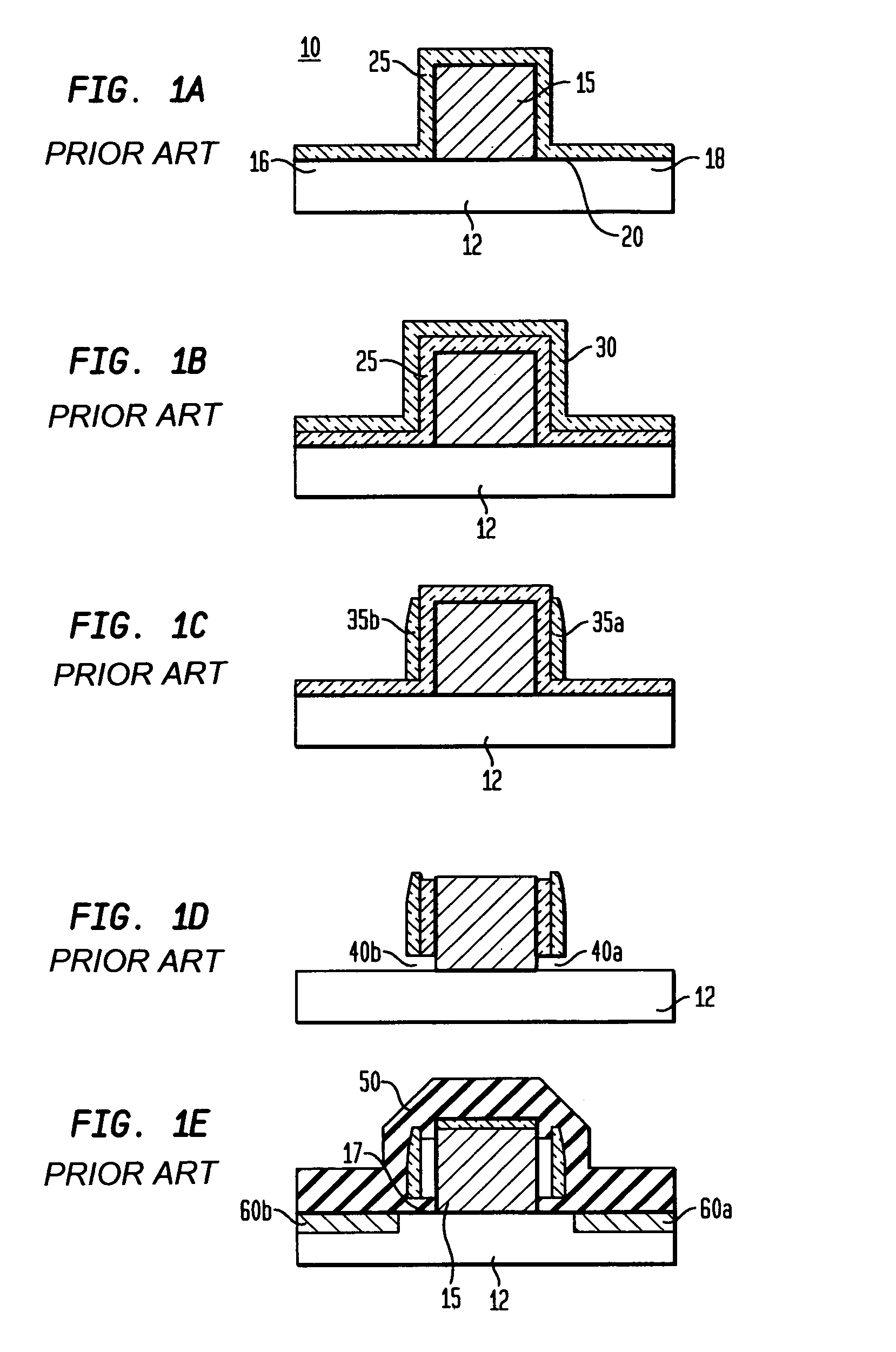
[0024]FIG. 2(a) illustrates an initial structure that is employed in the present invention. Specifically, the initial structure shown in FIG. 2(a) comprises a semiconductor substrate 12 having a patterned gate stack 15 formed on portions of the semiconductor substrate. In accordance with the present invention, each patterned gate stack includes a gate dielectric 20, gate conductor 15 formed atop the gate dielectric, and an additional dielectr...


PUM


Abstract

A method for forming a CMOS device in a manner so as to avoid dielectric layer undercut during a pre-silicide cleaning step is described. During formation of CMOS device comprising a gate stack on a semiconductor substrate surface, the patterned gate stack including gate dielectric below a conductor with vertical sidewalls, a dielectric layer is formed thereover and over the substrate surfaces. Respective nitride spacer elements overlying the dielectric layer are formed at each vertical sidewall. The dielectric layer on the substrate surface is removed using an etch process such that a portion of the dielectric layer underlying each spacer remains. Then, a nitride layer is deposited over the entire sample (the gate stack, the spacer elements at each gate sidewall, and substrate surfaces) and subsequently removed by an etch process such that only a portion of said nitride film (the “plug”) remains. The plug seals and encapsulates the dielectric layer underlying each said spacer, thus preventing the dielectric material from being undercut during the subsequent pre-silicide clean process. By preventing undercut, this invention also prevents the etch-stop film (deposited prior to contact formation) from coming into contact with the gate oxide. Thus, the integration of thin-spacer transistor geometries, which are required for improving transistor drive current, is enabled.

Description

BACKGROUND OF INVENTION[0001]The present invention relates to complementary metal oxide semiconductor (CMOS) devices, and more particularly to a process and structure for forming a metal oxide semiconductor field effect transistor (MOSFET) implementing thin sidewall spacer geometries.[0002]FIGS. 1(a)–1(e) depict cross-section views of a portion of a semiconductor device manufactured in accordance with conventional processing techniques. As shown in FIG. 1(a), a semiconductor device 10 is formed on a wafer. The device includes a substrate 12 and a patterned gate stack 15 formed thereon. Each patterned gate stack 15 may be formed of a gate material such as polycrystalline silicon, for example, and as conventionally known, the gate 15 is formed on a thin gate dielectric layer 20 previously formed on top of the substrate 12. Prior to the formation of low resistivity cobalt, titanium, or nickel silicide contacts with active device regions 16, 18 and gate 15 of the semiconductor device 10...

Claims


Application Information

Patent Timeline
Patent Type & Authority Patents(United States)
IPC IPC(8): H01L21/8238H01L21/28H01L21/311H01L21/3205H01L21/336H01L23/52H01L27/092H01L29/417H01L29/423H01L29/49H01L29/78
CPCH01L21/02063H01L21/31116H01L21/823835H01L21/823864H01L29/665H01L29/6653H01L29/6656H01L2924/0002H01L2924/00H01L21/18
Inventor AJMERA, ATUL C.BRYANT, ANDRESGILBERT, PERCY V.GRIBELYUK, MICHAEL AMACIEJEWSKI, EDWARD P.MO, RENEE T.NARASIMHA, SHREESH
Owner AURIGA INNOVATIONS INC
Why Eureka
Try Eureka