Superconducting disk resonator

a superconducting disk and resonator technology, applied in the direction of resonators, waveguides, electrical devices, etc., can solve the problems of increasing loss, creating obstacles to realizing power efficiency, and high power needed to transmit high frequency signals, so as to prevent the occurrence of a notch and achieve suitable frequency characteristics

a superconducting disk and resonator technology, applied in the direction of resonators, waveguides, electrical devices, etc., can solve the problems of increasing loss, creating obstacles to realizing power efficiency, and high power needed to transmit high frequency signals, so as to prevent the occurrence of a notch and achieve suitable frequency characteristics

US20080274899A1Inactive Publication Date: 2008-11-06FUJITSU LTD

Image

  • Superconducting disk resonator
  • Superconducting disk resonator
  • Superconducting disk resonator

Examples


Embodiment Construction

[0034]In the following, preferred embodiments of the present invention are described with reference to the accompanying drawings.

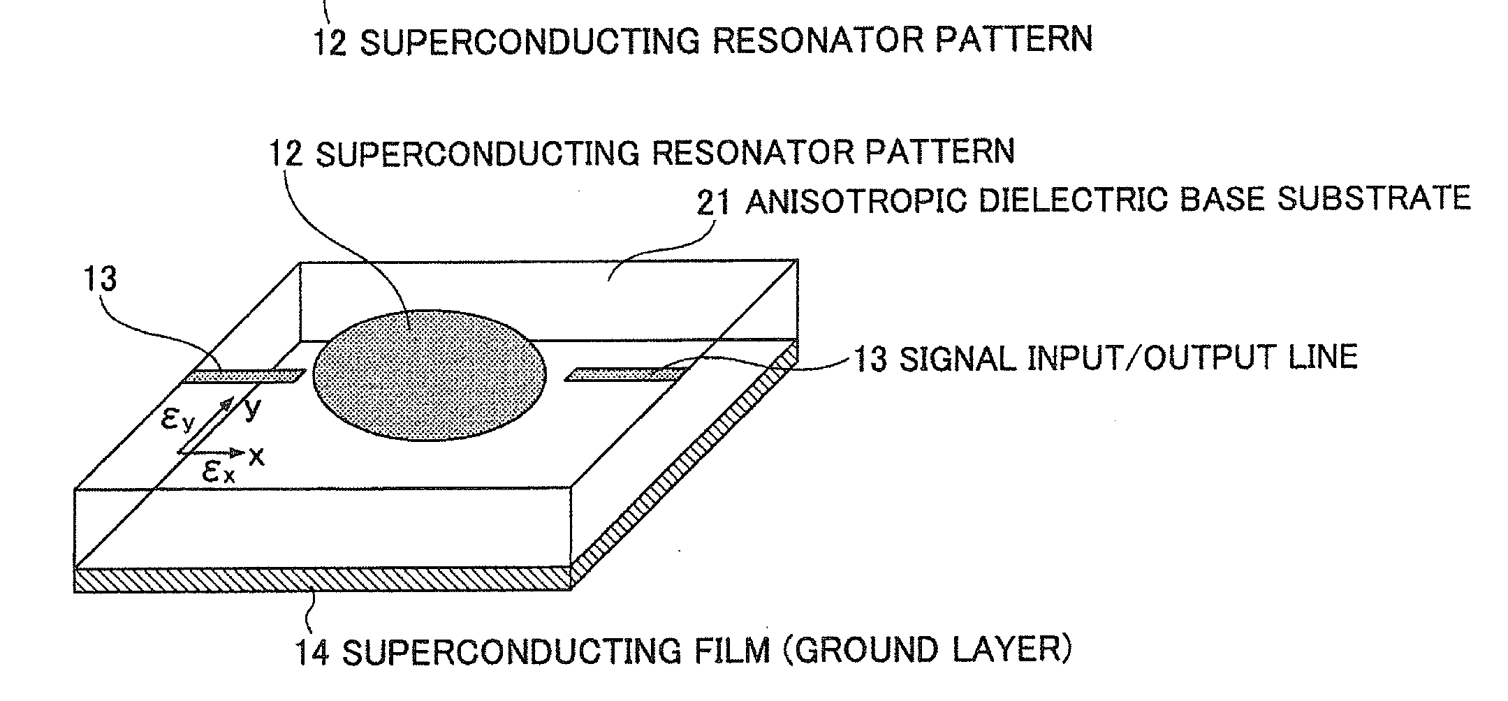
[0035]FIG. 3A is a plan view and FIG. 3B is a perspective view of a superconducting disk resonator 10 according to an embodiment of the present invention. FIG. 3C is a diagram showing frequency characteristics of the superconducting resonator 10 of FIGS. 3A and 3B.

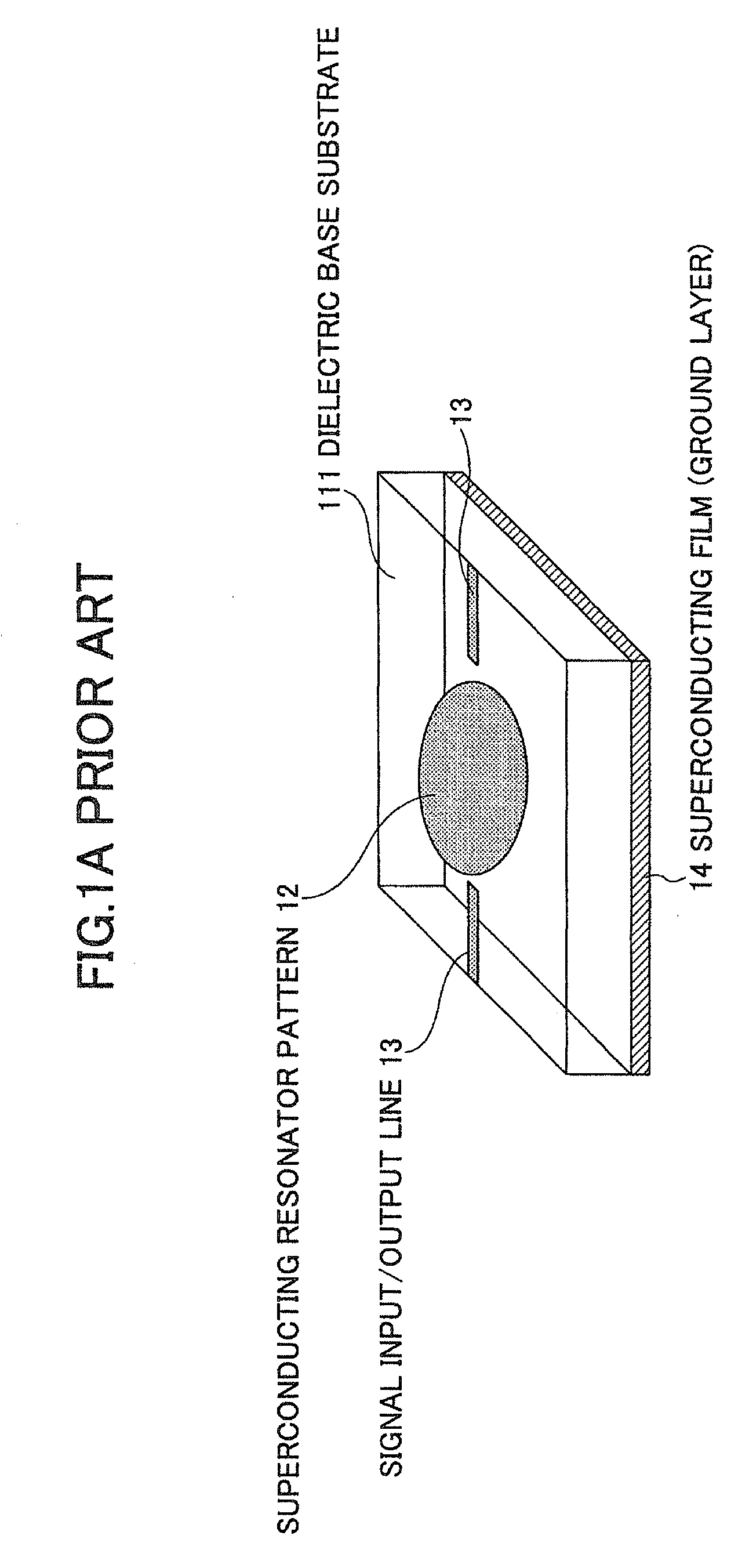
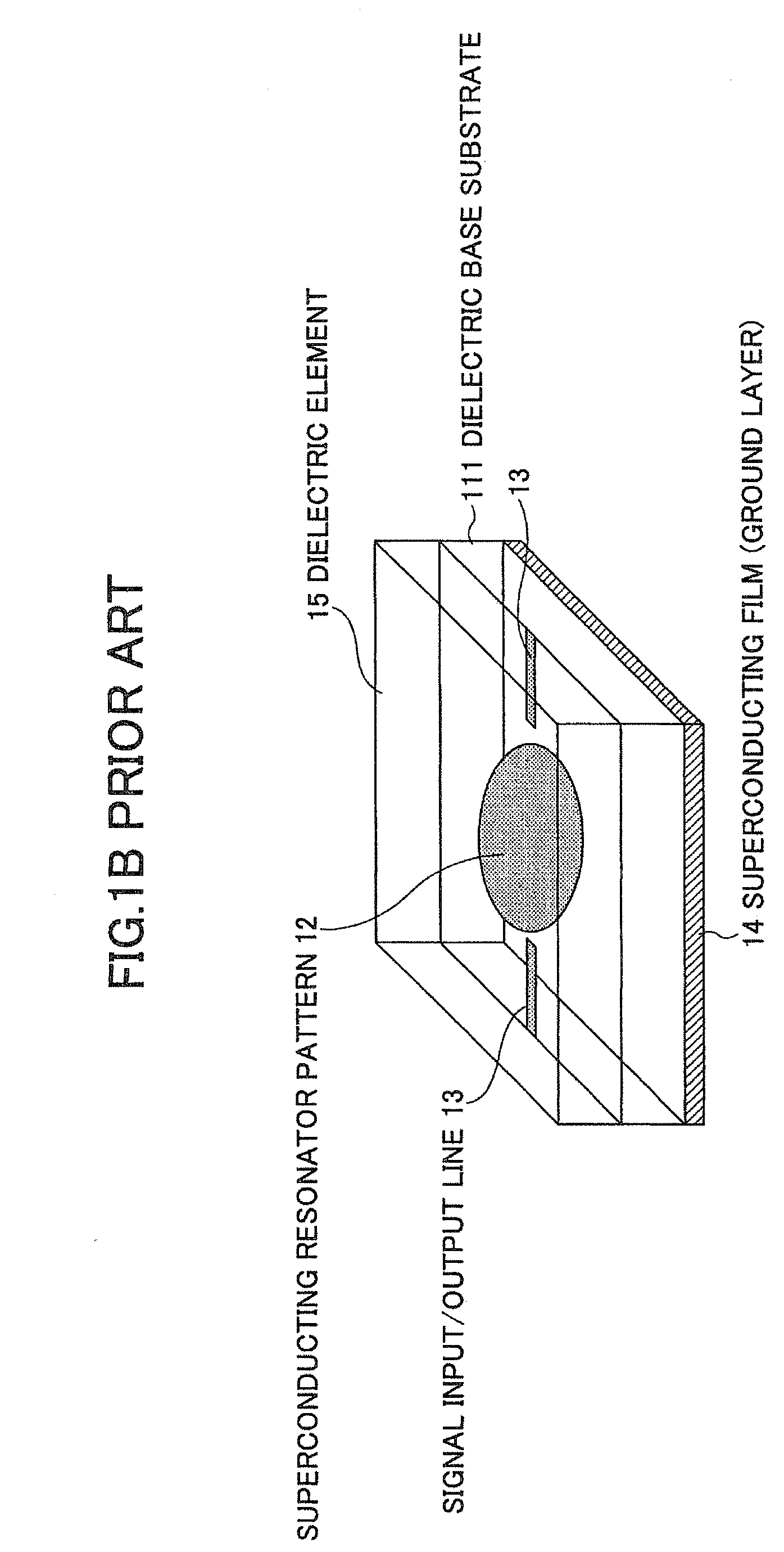
[0036]The illustrated superconducting disk resonator 10 includes an anisotropic dielectric base substrate 21, a disk type resonator pattern (signal layer) 12 that is made of superconducting material and is formed on the dielectric base substrate 21, a pair of signal input / output lines 13 extending in a straight line towards the superconducting resonator pattern 12. The superconducting disk resonator 10 also has a superconducting film (ground layer) 14 arranged on the rear face of the dielectric base substrate 21. In one example, YBCO (Y—Ba—Cu—O) material may be used as the superconducting materia...


PUM


Abstract

A superconducting disk resonator is disclosed that includes a dielectric base substrate having dielectric anisotropy, a disk type superconducting resonator pattern that is formed on the dielectric base substrate with superconducting material, and a pair of signal input / output lines arranged on the dielectric base substrate and extending in a straight line towards the disk type superconducting resonator pattern. The direction of dielectric anisotropy of the dielectric base substrate is oriented at ±90 degrees with respect to an extending direction of the pair of signal input / output lines.

Description

BACKGROUND OF THE INVENTION[0001]1. Field of the Invention[0002]The present invention relates to a superconducting disk resonator that is used in a transmitting front end such as a transmitting filter or antenna in the field of mobile communication and broadcasting.[0003]2. Description of the Related Art[0004]In view of the growing popularity and development of mobile phones, high-speed high-capacity transmission techniques are in great demand. A superconductor is favorably considered for application to a filter of a base station of a mobile communication system since it has relatively low surface resistance even in a high frequency domain compared to a conventional electrical conductor so that a low-loss high-Q value resonator may be realized.[0005]In the case of using a superconducting filter as a receiving side band filter, transmission loss may be reduced and accurate frequency blocking characteristics may be realized, for example. In the case of using the superconducting filter...

Claims


Application Information

Patent Timeline
06 Nov 2008
Publication
US20080274899A1
IPC
H01P1/203
CPC
H01P7/08; H01P7/10; H10N60/00
Inventors
AKASEGAWA, AKIHIKO; NAKANISHI, TERU