
Semiconductor Device

a technology of semiconductor devices and diodes, applied in the field of semiconductor devices, can solve the problems of increasing die costs, complex array patterns of islands and leads, and degrading cooling performance of elements, so as to reduce costs, simplify the work of mounting diodes, and suppress the effect of a temperature rise in the semiconductor devi

Active Publication Date: 2008-11-27
MAHLE INT GMBH
View PDF1 Cites 10 Cited by
  • Summary
  • Abstract
  • Description
  • Claims
  • Application Information

AI Technical Summary

Benefits of technology

[0012]It is an object of the present invention to provide a semiconductor device capable of being mounted on a circuit board in a well-balanced manner.
[0013]It is another object of the present invention to provide a semiconductor device in which it is possible to make a design change, such as a change in the dimensions of islands, without changing the array of leads and a distance therebetween.
[0014]It is yet another object of the present invention to provide a semiconductor device the cooling performance of which can be improved by reducing the number of semiconductor chips to be buried in one resin-seal portion to suppress a temperature rise.

Problems solved by technology

Furthermore, the semiconductor device becomes hot whether it takes a single-in-line form or a dual-in-line form since all heat-evolving elements comprising the semiconductor device are buried in one resin-seal portion, thereby resulting in the problem that the cooling performance of the elements degrades.
Still furthermore, in a conventional semiconductor device, it has been unavoidable that the array patterns of islands and leads become complicated if there are an increased number of islands since leads to be provided for each island must be led to an end of a lead frame in its width direction.
Accordingly, the structure of a punching die becomes complicated in a case where the lead frame is formed by punching, thereby resulting in the problem that the costs of the die increase.
Although a semiconductor device comprising a power circuit has been taken as an example above to explain problems with the semiconductor device, the same problems as described above arise also in a semiconductor device comprising an electronic circuit other than power circuits if the semiconductor device has a single-in-line construction or a dual-in-line construction.

Method used


Image

  • Semiconductor Device
  • Semiconductor Device
  • Semiconductor Device

Examples


Embodiment Construction

[0066]Preferred embodiments of the present invention will hereinafter be described in detail with reference to the accompanying drawing.

[0067]In the present embodiment, there is taken as an example a semiconductor device comprising a power circuit used for a short-circuit type voltage regulator circuit for controlling a voltage supplied from a three-phase magnetic AC generator driven by a motor, such as an engine, to a DC load so that the voltage is kept to within a preset range.

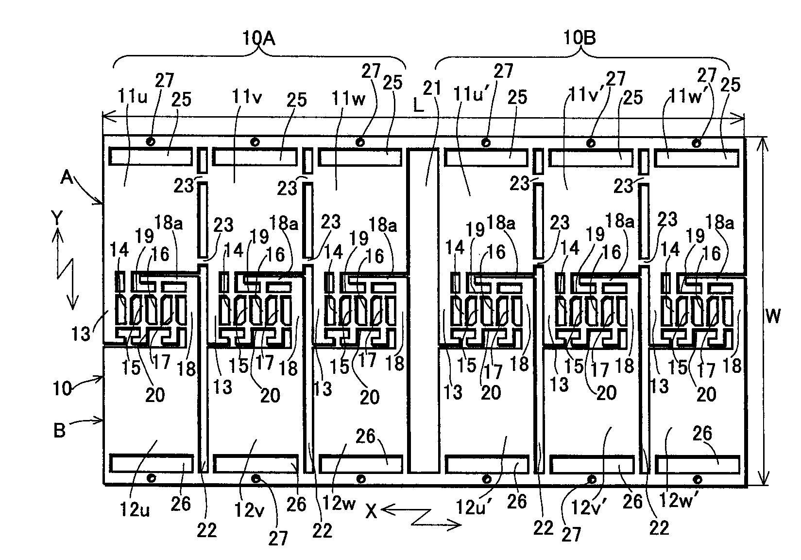
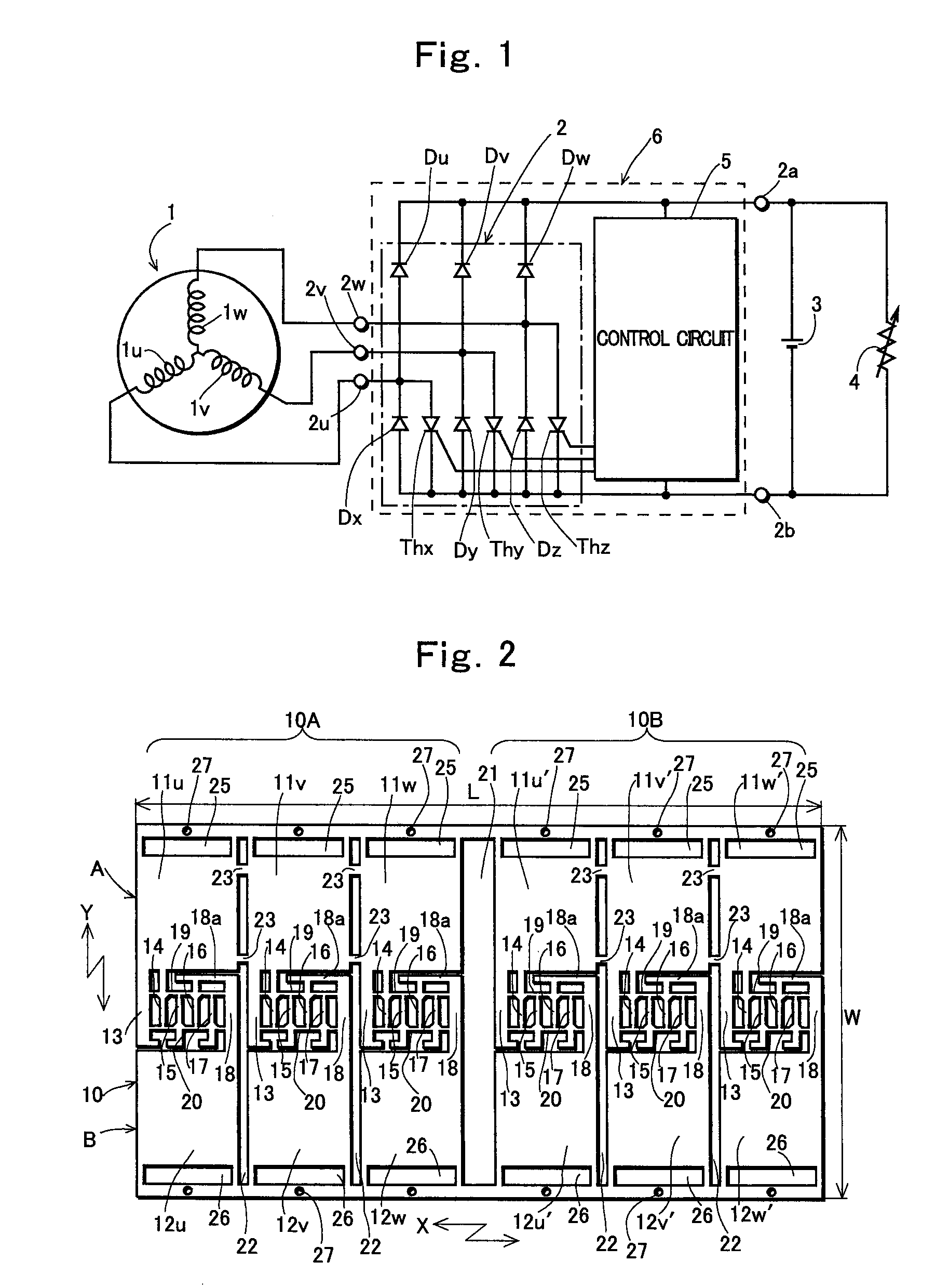
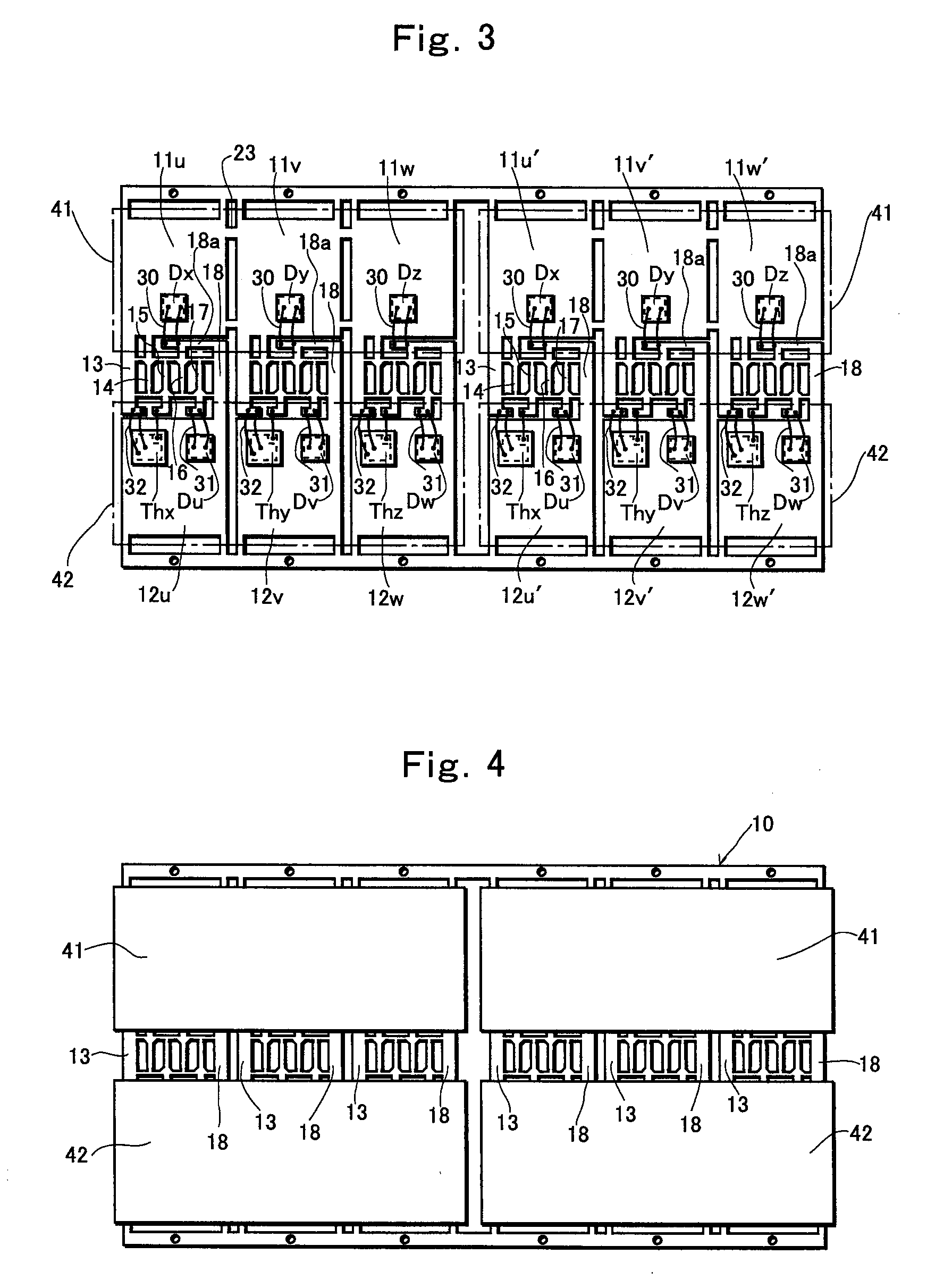
[0068]In FIG. 1, 1 denotes a three-phase magnetic AC generator driven by a motor, where the generator is comprised of a magnetic rotator (not illustrated) mounted on the rotating shaft of the motor and a stator having three-phase armature coils 1u to 1w. 2 denotes a semiconductor device whereto the present invention is applied, where the semiconductor device comprises a short-circuit type voltage regulator circuit (a part in which a large current flows) having a rectification function.

[0069]The illustrated s...


PUM


Abstract

A semiconductor device having a plurality of semiconductor chips mounted on a lead frame (10) and required portions covered with seal portions in which: the plurality of semiconductor chips are divided into a first group of semiconductor chips (Dx to Dz) and a second group of semiconductor chips (Du to Dw and Thx to Thz); both groups of semiconductor chips are mounted on the lead frame (10) at a distance from each other; the seal portions are comprised of first and second resin-seal portions (41 and 42) which cover the first and second groups of semiconductor chips, respectively, along with required portions of the lead frame; both resin-seal portions are mechanically coupled with each other by coupling portions; and a group of read terminals respectively connected to circuits within the first resin-seal portion and circuits within the second resin-seal portion are led out through a gap between the first resin-seal portion (41) and the second resin-seal portion (42).

Description

TECHNICAL FIELD OF THE INVENTION[0001]The present invention relates to a semiconductor device having a structure that a plurality of semiconductor chips are mounted on a lead frame and the plurality of semiconductor chips and required portions of the lead frame to be covered are covered with seal portions.PRIOR ART OF THE INVENTION[0002]In a semiconductor device where a predetermined circuit is comprised using a plurality of semiconductor chips, the plurality of semiconductor chips are mounted on an island of a lead frame, and each semiconductor chip and the inner leads of the lead frame are connected to each other using wires or the like. In addition, seal portions made of a resin-molded material are formed so as to cover the islands of the lead frame, the semiconductor chips mounted on the islands and the inner leads, in order to safeguard the semiconductor chips and the wired parts.[0003]This type of semiconductor device is used in a variety of fields. For example, in the field o...

Claims


Application Information

Patent Timeline
IPC IPC(8): H01L23/495
CPCH01L23/49555H01L23/49562H01L23/49575H01L25/072H01L2224/48091H01L2924/13091H01L2224/48247H01L2924/1301H01L24/48H01L2924/01066H01L2924/00014H01L2924/00H01L2924/181H01L2224/0603H01L2924/00012H01L2224/45099H01L2224/45015H01L2924/207
Inventor MURAMATSU, SHUICHISUZUKI, HIDETOSHISATO, TOMOYUKIHARA, KAZUOYAMAZAKI, MOTOKIASARI, MASAKIYAMAGUCHI, HIROFUMI
Owner MAHLE INT GMBH
Learn More