Mask mold, manufacturing method thereof, and method for forming large-sized micro pattern using mask mold

a manufacturing method and mask mold technology, applied in the field of mask molds, can solve the problems of increasing manufacturing time and cost, increasing the imprinting process time, and increasing geometrical progression or the inability to manufacture a large-sized micro-pattern larger than a predetermined size at one time, and achieving the effect of low cost and stitching errors

Inactive Publication Date: 2008-12-04
SAMSUNG ELECTRONICS CO LTD
View PDF8 Cites 25 Cited by
  • Summary
  • Abstract
  • Description
  • Claims
  • Application Information

AI Technical Summary

Benefits of technology

[0013]Accordingly, it is an aspect of the embodiment to provide a mask mold, a manufacturing method of the mask mold, and a method for forming a large-sized micro pattern using the manufactured mask mold, in which the size of a nano-level micro pattern can be enlarged using a simple method with low cost and interference and stitching errors between cells forming a large area can be minimized.

Problems solved by technology

When the size of a micro pattern is enlarged using the wafer, the cost increases in geometrical progression or a large-sized micro pattern larger than a predetermined size cannot be manufactured due to limitation in equipments.
Further, in a case in which a pattern to be transferred requires a three dimensional complicated process, the manufacturing time and cost increase in order to enlarge the size of the pattern at one time.
However, as the size of a substrate becomes larger, the imprinting process time also increases.
Further, alignment errors between cells (small areas in which patterns are formed during the imprinting process using the small mold) frequently occur due to the continuous repeating of the small mold.
That is, in the case of enlarging the size of the micro pattern using the step-and-repeat scheme, when alignment errors between cells occur or the dispensing amount of the resist is not precisely controlled, interference and stitching errors (an area without patterns occurs or undesired patterns are formed) between cells may occur.

Method used


Image

  • Mask mold, manufacturing method thereof, and method for forming large-sized micro pattern using mask mold
  • Mask mold, manufacturing method thereof, and method for forming large-sized micro pattern using mask mold
  • Mask mold, manufacturing method thereof, and method for forming large-sized micro pattern using mask mold

Examples


Embodiment Construction

[0036]Reference will now be made in detail to the embodiment, an example of which is illustrated in the accompanying drawings, wherein like reference numerals refer to the like elements throughout. The embodiment is described below to explain the present invention by referring to the figures.

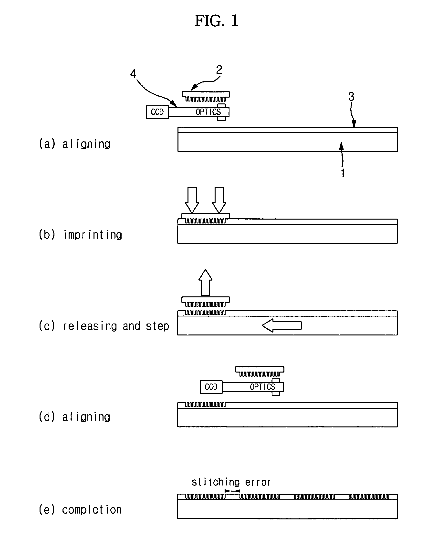
[0037]FIGS. 2A to 2H are sectional views illustrating the procedure for manufacturing mask molds and forming a large-sized micro pattern using the manufactured mask molds according to an embodiment. FIG. 3 is a view illustrating arrangement of the mask molds for forming the large-sized micro pattern and a repeated imprinting process according to an embodiment.

[0038]Hereinafter, an embodiment will be described in detail with reference to FIGS. 2A to 2H and FIG. 3.

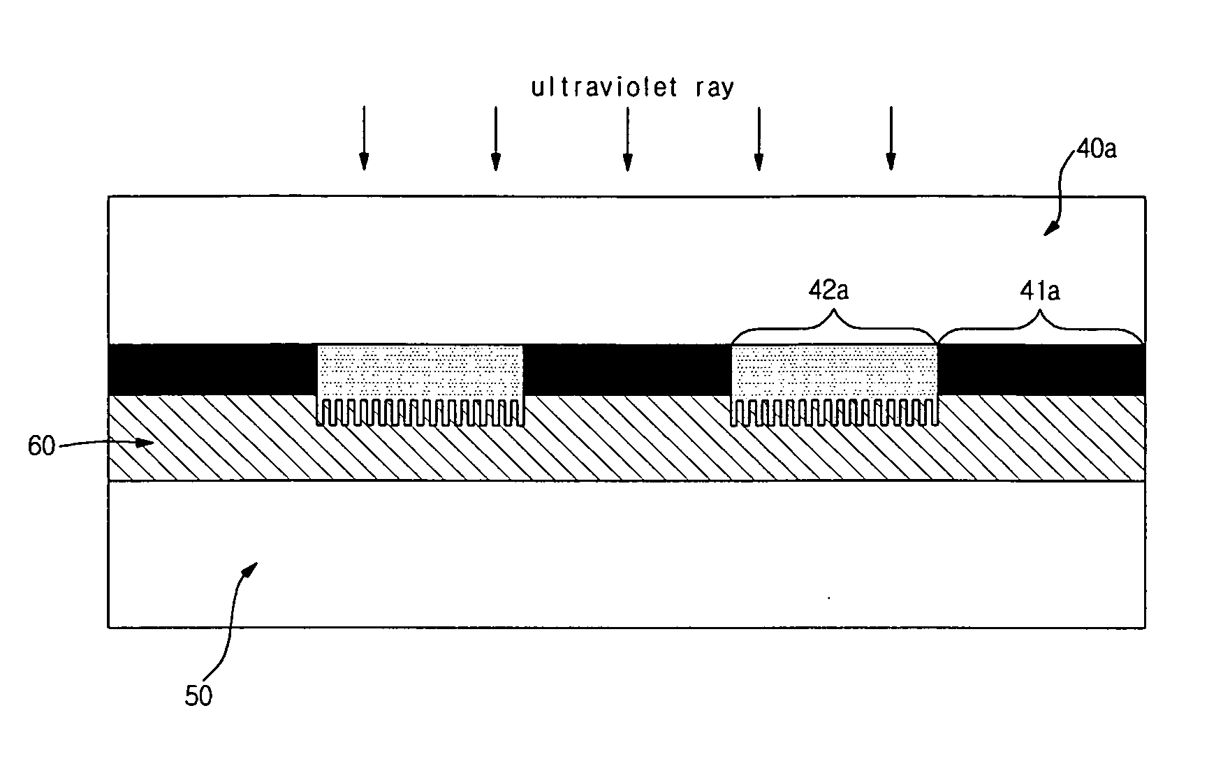
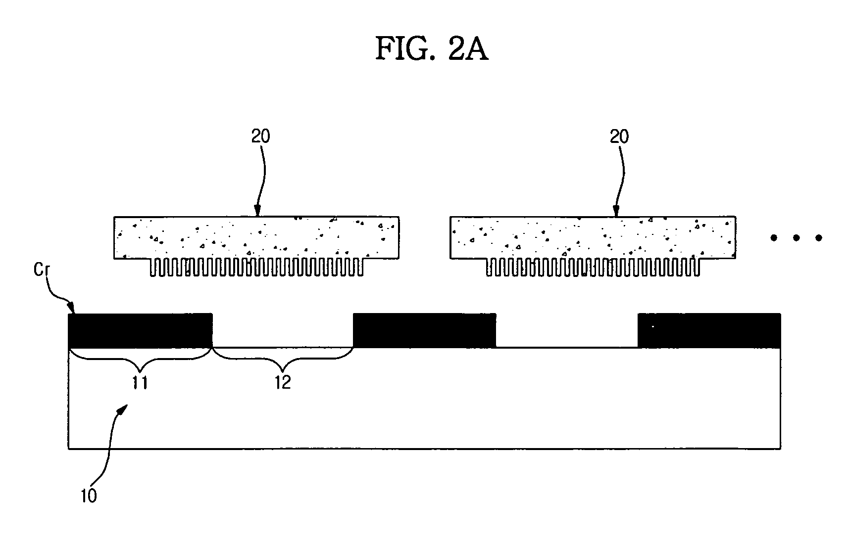
[0039]FIGS. 2A to 2C shows the method for manufacturing the mask molds 40a and 40b of FIG. 2G. In order to manufacture the mask molds 40a and 40b, a plurality of small molds 20 having micro patterns engraved through the e-beam lithograph...


PUM

PropertyMeasurementUnit
angleaaaaaaaaaa
shapeaaaaaaaaaa
areaaaaaaaaaaa

Abstract

Disclosed are a mask mold, a manufacturing method thereof, and a method for forming a large-sized micro pattern using the manufactured mask mold, in which the size of a nano-level micro pattern can be enlarged using a simple method with low cost and interference and stitching errors between cells forming a large area can be minimized. The method for manufacturing the mask mold includes the operations of coating resist on a mask or a plurality of small molds having an engraved micro pattern, pressing the small molds to imprint the micro pattern on the resist, curing the resist, and releasing the small molds from the resist.

Description

CROSS-REFERENCE TO RELATED APPLICATIONS[0001]This application claims the benefit of Korean Patent Application No. 10-2007-0053228, filed on May 31, 2007, in the Korean Intellectual Property Office, the disclosure of which is incorporated herein by reference.BACKGROUND[0002]1. Field[0003]One or more embodiments relate to a mask mold, a manufacturing method thereof, and a method for forming a large-sized micro pattern using the manufactured mask mold. More particularly, the embodiments relate to a mask mold, a manufacturing method of the mask mold, and a method for forming a large-sized micro pattern using the manufactured mask mold, in which the size of a micro pattern engraved on a small mold can be enlarged using a plurality of mask molds which can be manufactured using a simple method.[0004]2. Description of the Related Art[0005]According to nano-imprint technology, a substrate coated with thermoplastic resin or photocurable resin is pressed by a mold having a micro pattern with a...

Claims


Application Information

Patent Timeline
Patent Type & Authority Applications(United States)
IPC IPC(8): G03F1/14B05D3/06B29C33/38B29C59/02B81C99/00G03F7/20H01L21/027
CPCB82Y10/00B82Y40/00G03F7/0002B41D7/00G03F7/2012Y10S977/887
Inventor KIM, JEONG GILCHO, YOUNG TAESIM, YOUNG SUKCHO, SUNG HOONLEE, SUK WONPARK, SEON MIKWON, SINSEO, JUNG WOOPARK, JUNG WOOCHO, SUNG WOO
Owner SAMSUNG ELECTRONICS CO LTD
Why Eureka
Try Eureka