

Non-volatile semiconductor memory device
- Summary
- Abstract
- Description
- Claims
- Application Information
AI Technical Summary
Problems solved by technology
Method used
Image

Examples
first embodiment
[0034]An embodiment in the present invention is described below.
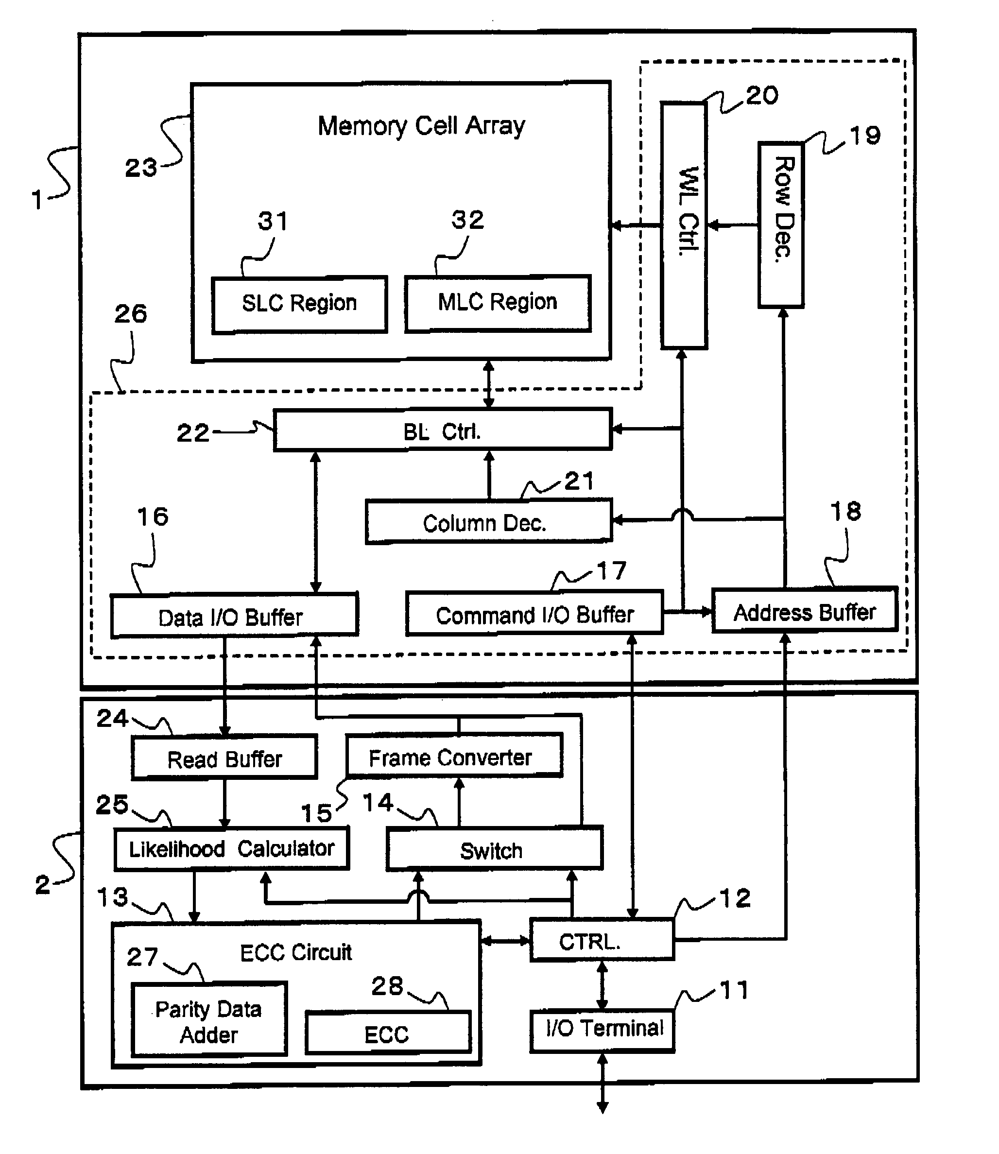
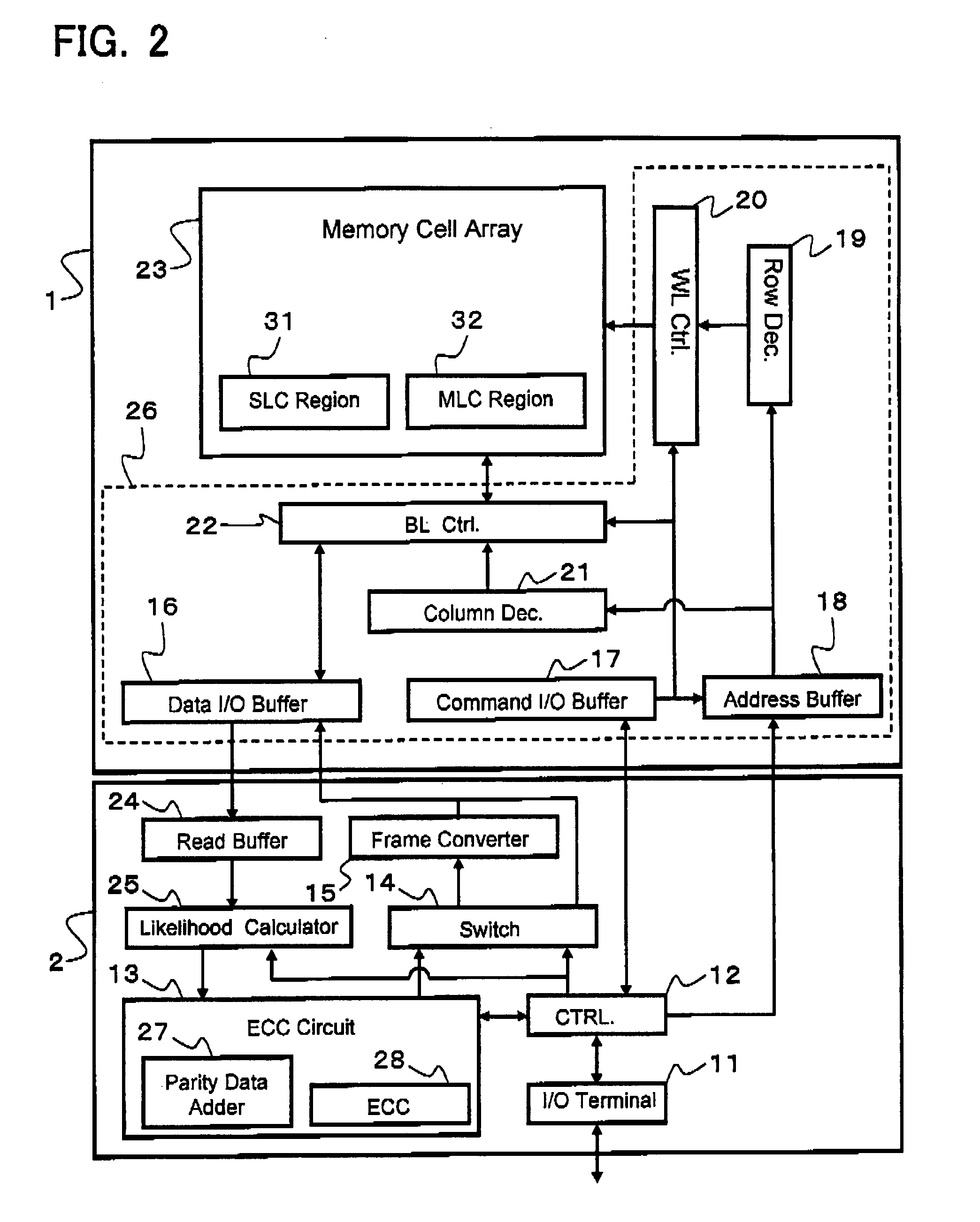
[0035]FIG. 2 is a block diagram of a 3-bit multi-level storage NAND cell-type flash memory, which is a non-volatile semiconductor memory device in the present embodiment.
[0036]The 3-bit multi-level storage NAND cell-type flash memory in the present embodiment comprises a memory section 1, and a control section 2 for controlling the memory section 1.
[0037]The memory section 1 includes a data I / O buffer 16, a command I / O buffer 17, an address buffer 18, a row decoder 19, a word line controller 20, a column decoder 21, a bit line controller 22, and a memory cell array 23. A programming circuit 26 includes the data I / O buffer 16, the command I / O buffer 17, the address buffer 18, the row decoder 19, the word line controller 20, the column decoder 21, and the bit line controller 22.
[0038]The memory cell array 23 includes memory cells arrayed in matrix for data storage. Namely, the memory cell array 23 includes a plurality of ...
second embodiment
[0106]A second embodiment has a different arrangement, in the ECC page data, of subframe data formed at the frame converter 15.
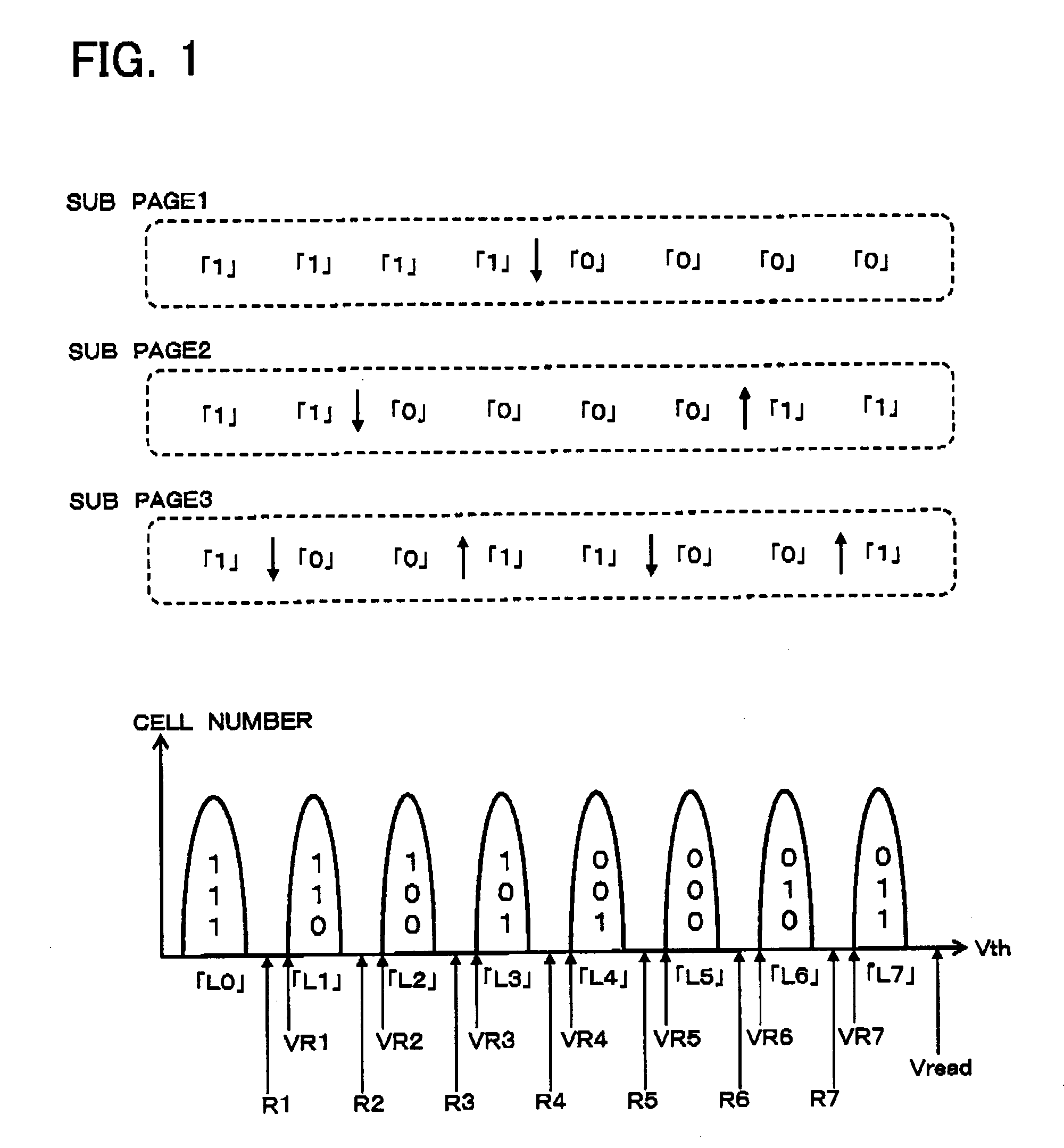
[0107]Specifically, the pieces of subframe data divided are arranged in pages in the MLC region 32 as shown in FIG. 12. The ECC page data in the present embodiment includes three sub-pages each composed of k ECC frames. This is because the multi-level memory in the MLC region 32 can store three bits in one memory cell and accordingly the bits in the multi-level memory can configure respective sub-pages. Specifically, as shown in FIG. 12, k pieces of frame data A, k pieces of frame data B, and k pieces of frame data C as ECC frames are integrated to form the ECC page data in the MLC region 32. Therefore, the ECC page data includes frame data A1-Ak, frame data B1-Bk, and frame data C1-Ck.
[0108]The frame data A1 is divided into three to form subframe data including data A1(1), subframe data including data A1(2), and subframe data including data A1(3) and parity...
third embodiment
[0112]A third embodiment has a different arrangement, in the ECC page data, of sub-page data formed at the frame converter 15.
[0113]Specifically, the pieces of subframe data divided are arranged in pages in the MLC region 32 as shown in FIG. 13. The ECC page data in the present embodiment includes three sub-pages each composed of k ECC frames. This is because the multi-level memory in the MLC region 32 can store three bits in one memory cell and accordingly the bits in the multi-level memory can configure respective sub-pages. Specifically, as shown in FIG. 13, k pieces of frame data A, k pieces of frame data B, and k pieces of frame data C as ECC frames are integrated to form the ECC page data in the MLC region 32. Therefore, the ECC page data includes frame data A1-Ak, frame data B1-Bk, and frame data C1-Ck.
[0114]The frame data A1, A2, A3 or the like is divided into three to form pieces of subframe data in the same manner as in the second embodiment.
[0115]The pieces of subframe da...
PUM
 Abstract
Description
Claims
Application Information