Graphene-based transistor

Active Publication Date: 2009-01-22
GLOBALFOUNDRIES US INC
View PDF6 Cites 267 Cited by
  • Summary
  • Abstract
  • Description
  • Claims
  • Application Information

AI Technical Summary

Benefits of technology

[0012]The present invention addresses the needs described above by providing field effect transistor structures employing a graphene layer for the channel and having source and drain regions formed

Problems solved by technology

A free-standing graphene structure is theoretically stable only in a two-dimensional space, which implies that a planar graphene structu

Method used


Image

  • Graphene-based transistor
  • Graphene-based transistor
  • Graphene-based transistor

Examples


first embodiment

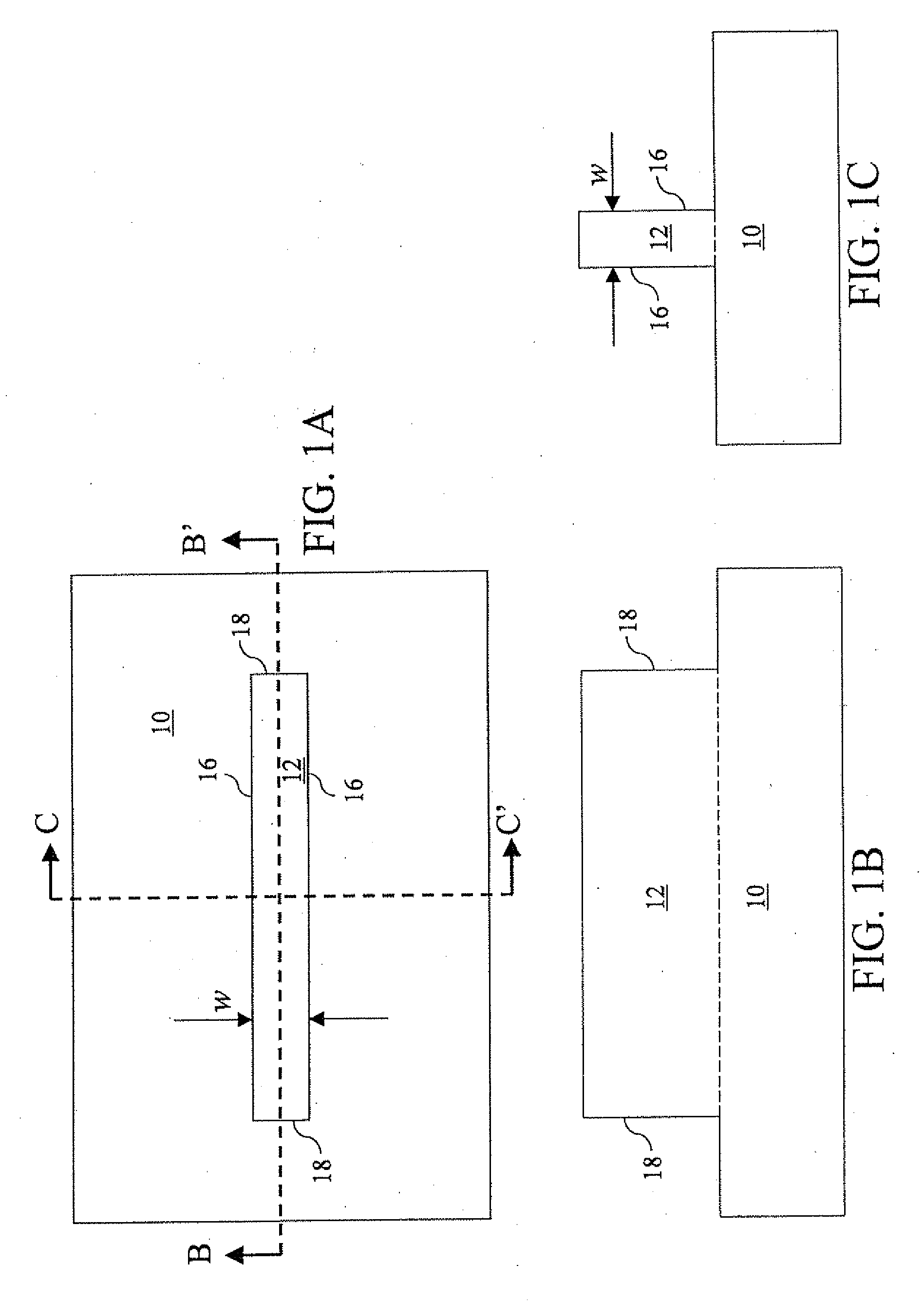
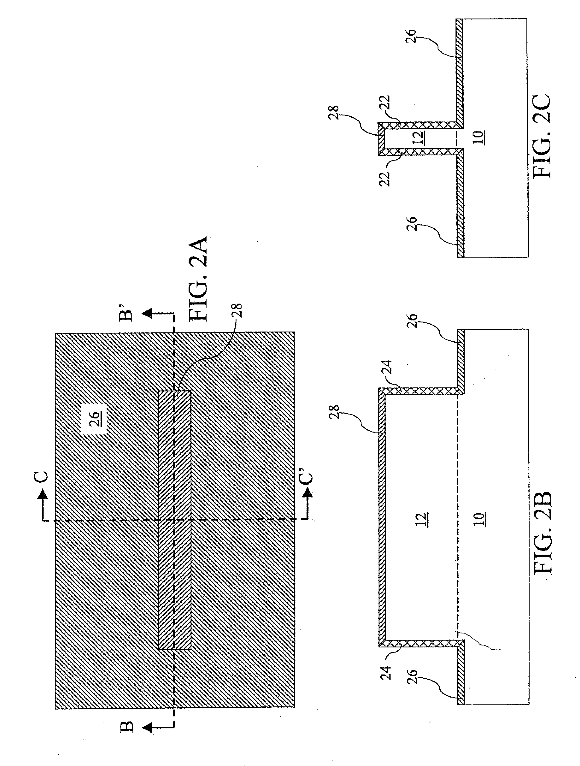
[0066]According to the present invention, a silicon carbide fin 12 formed on a silicon carbide substrate 10 is shown in FIGS. 1A-1C. The silicon carbide fin 12 is formed out of the silicon carbide substrate 10 by lithographic patterning and etching. For example, a photoresist (not shown) may be applied over a top surface of a planar initial silicon carbide substrate (not shown). After a lithographic patterning of the photoresist, the pattern in the photoresist is transferred into the planar initial silicon carbide substrate to form the silicon carbide fin 12 and the silicon carbide substrate 10 underneath. The portion of the silicon carbide substrate 10 that is covered by the photoresist corresponds to the silicon carbide fin 12. The interface between the silicon carbide fin 12 and the silicon carbide substrate 10 is marked by dotted lines in FIGS. 1B and 1C.

[0067]Preferably, the silicon carbide fin 12 comprises a first pair of sidewalls 16 that are substantially parallel to each ot...

second embodiment

[0084]According to the present invention, a trench 11 having a substantially flat bottom surface 13 and a pair of trench sidewalls 17 is formed in a silicon carbide substrate 10 as shown in FIG. 12. The trench 11 is formed within the silicon carbide substrate 10 by lithographic patterning and etching. For example, a photoresist (not shown) may be applied over a planar top surface of the silicon carbide substrate 10 followed by a lithographic patterning of the photoresist. The pattern in the photoresist is transferred into the silicon carbide substrate 10 to form the silicon carbide fin 12. The portion of the silicon carbide substrate 10 that is not covered by the photoresist corresponds to the trench 11.

[0085]Preferably, the depth d of the trench 11 exceeds the depth of source and drain regions to be subsequently formed. The crystallographic orientations of the silicon carbide substrate 10 are chosen such that the substantially flat bottom surface 13 is conducive to formation of a g...

third embodiment

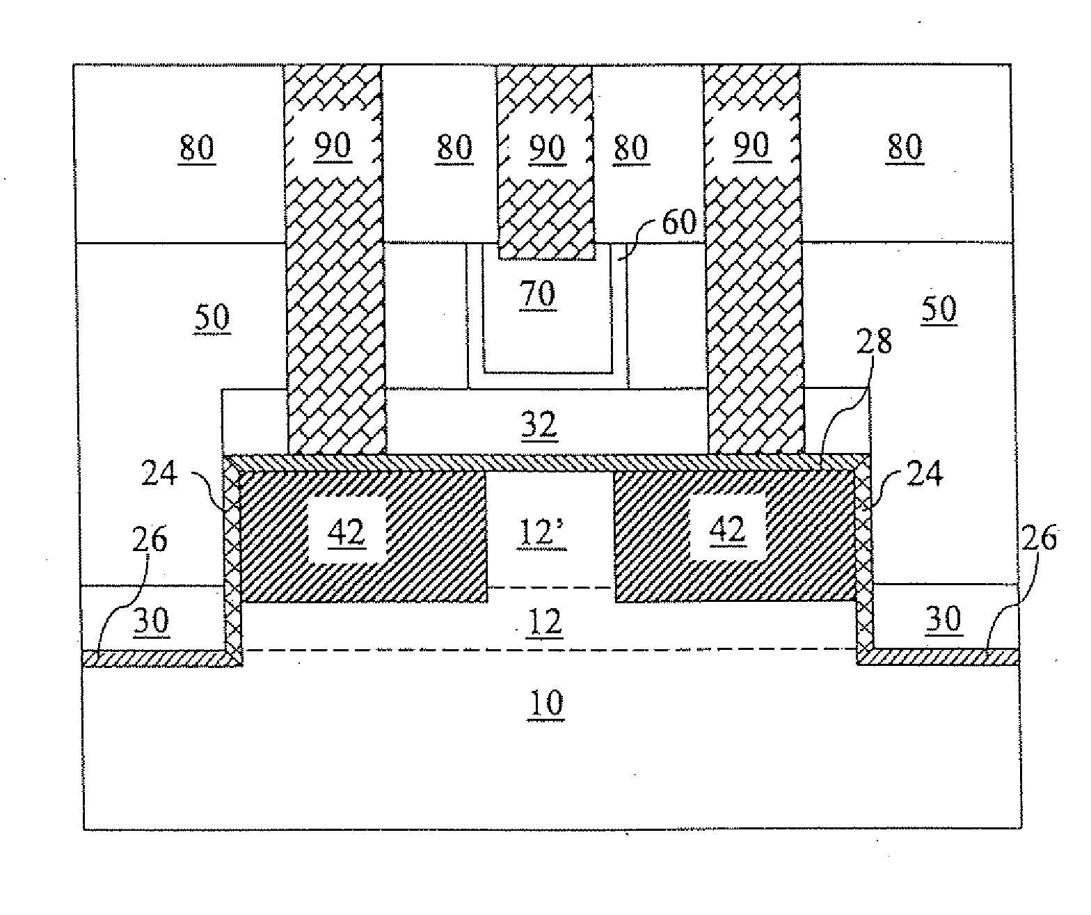
[0109]Referring to FIG. 31, an alternative field effect transistor structure according to the present invention does not contain the gate spacers 62.


PUM


Abstract

A graphene layer is formed on a surface of a silicon carbide substrate. A dummy gate structure is formed over the fin, in the trench, or on a portion of the planar graphene layer to implant dopants into source and drain regions. The dummy gate structure is thereafter removed to provide an opening over the channel of the transistor. Threshold voltage adjustment implantation may be performed to form a threshold voltage implant region directly beneath the channel, which comprises the graphene layer. A gate dielectric is deposited over a channel portion of the graphene layer. After an optional spacer formation, a gate conductor is formed by deposition and planarization. The resulting graphene-based field effect transistor has a high carrier mobility due to the graphene layer in the channel, low contact resistance to the source and drain region, and optimized threshold voltage and leakage due to the threshold voltage implant region.

Description

FIELD OF THE INVENTION[0001]The present invention relates to semiconductor structures, and particularly to graphene-based transistors and method of manufacturing the same.BACKGROUND OF THE INVENTION[0002]Graphene refers to a two-dimensional planar sheet of carbon atoms arranged in a hexagonal benzene-ring structure. A free-standing graphene structure is theoretically stable only in a two-dimensional space, which implies that a planar graphene structure does not exist in a free state, being unstable with respect to formation of curved structures such as soot, fullerenes, and nanotubes. However, a two-dimensional graphene structure has been demonstrated on a surface of a three-dimensional structure, for example, on the surface of a SiC crystal.[0003]Structurally, graphene has hybrid orbitals formed by sp2 hybridization. In the sp2 hybridization, the 2s orbital and two of the three 2p orbitals mix to form three sp2 orbitals. The one remaining p-orbital forms a pi-bond between the carbo...

Claims


Application Information

Patent Timeline
IPC IPC(8): H01L31/0312H01L21/337
CPCH01L29/1606H01L29/66795H01L29/78687H01L29/7781H01L29/785H01L29/66803
Inventor ANDERSON, BRENT A.NOWAK, EDWARD J.
Owner GLOBALFOUNDRIES US INC
Why Eureka
Try Eureka