Programmable memory array structure incorporating series-connected transistor strings and methods for fabrication and operation of same

a series-connected transistor and array structure technology, applied in the field of monolithic three-dimensional memory arrays, can solve the problem that memory cells are less desirable for a 3d memory

Active Publication Date: 2004-07-01
SANDISK TECH LLC
View PDF98 Cites 259 Cited by
  • Summary
  • Abstract
  • Description
  • Claims
  • Application Information

AI Technical Summary

Problems solved by technology

Such memory cells are less desirable for a 3D memory because they use many masks to produce a memory layer, and some use relatively high programming currents.

Method used


Image

  • Programmable memory array structure incorporating series-connected transistor strings and methods for fabrication and operation of same
  • Programmable memory array structure incorporating series-connected transistor strings and methods for fabrication and operation of same
  • Programmable memory array structure incorporating series-connected transistor strings and methods for fabrication and operation of same

Examples


Embodiment Construction

)

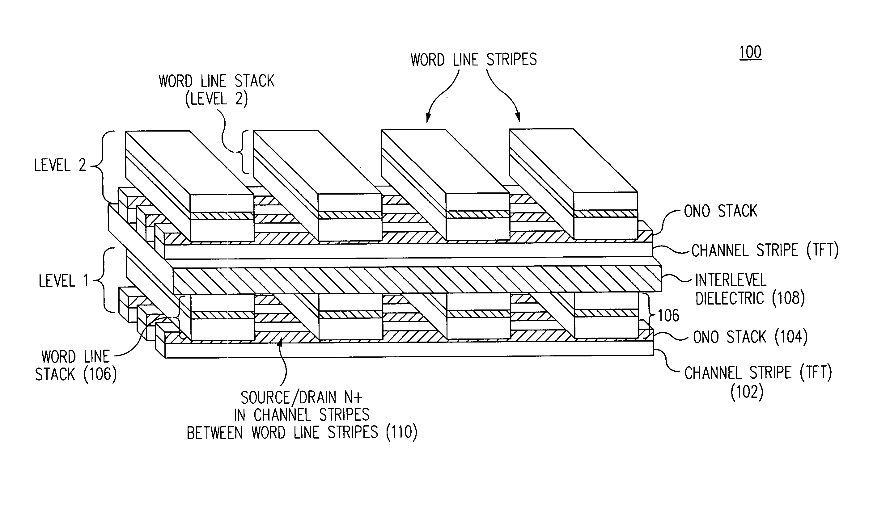
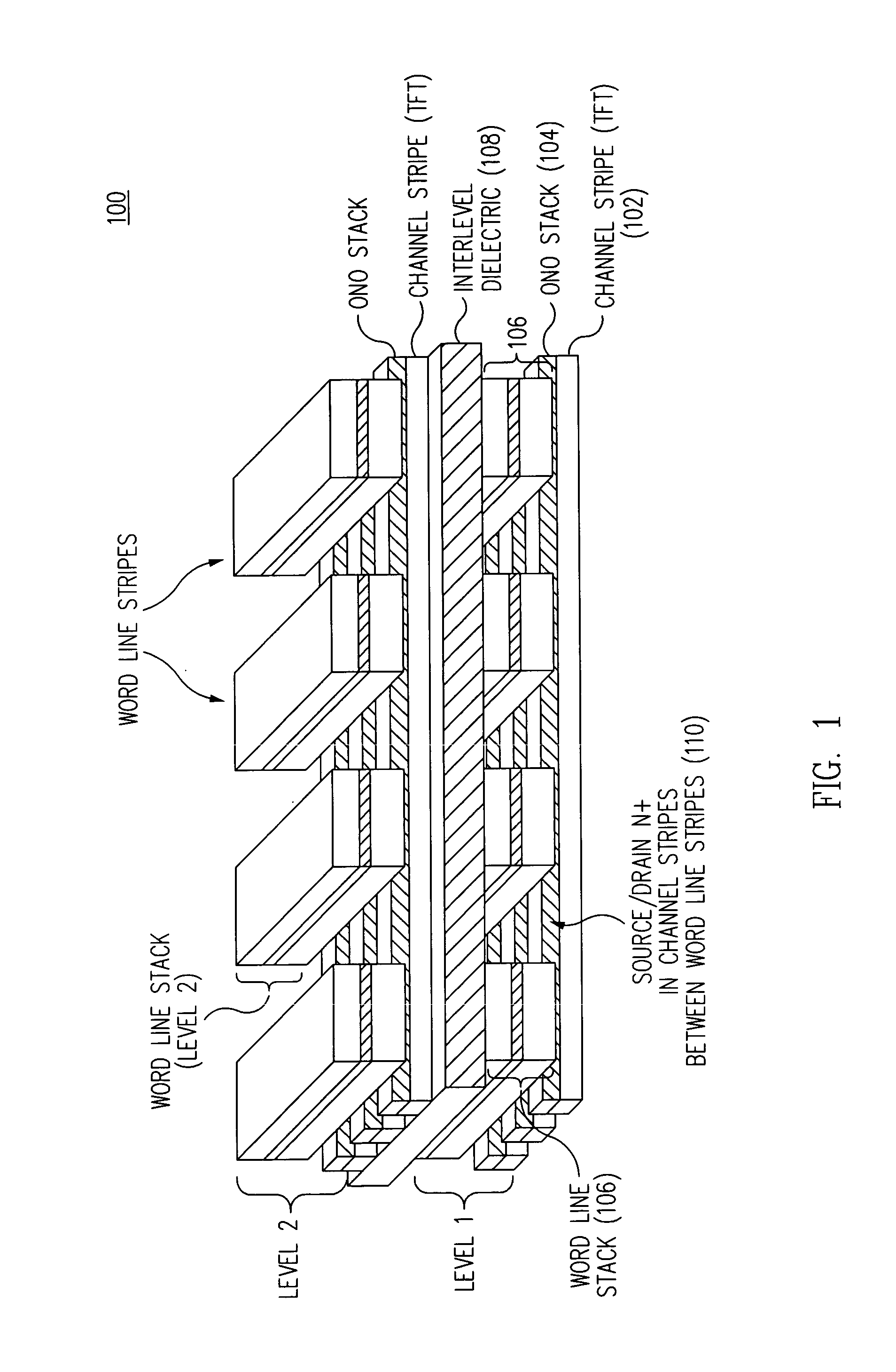
[0049] As used herein, an integrated circuit having a three-dimensional memory array is assumed to be a monolithic integrated circuit, rather than an assembly of more than one monolithic integrated circuit.

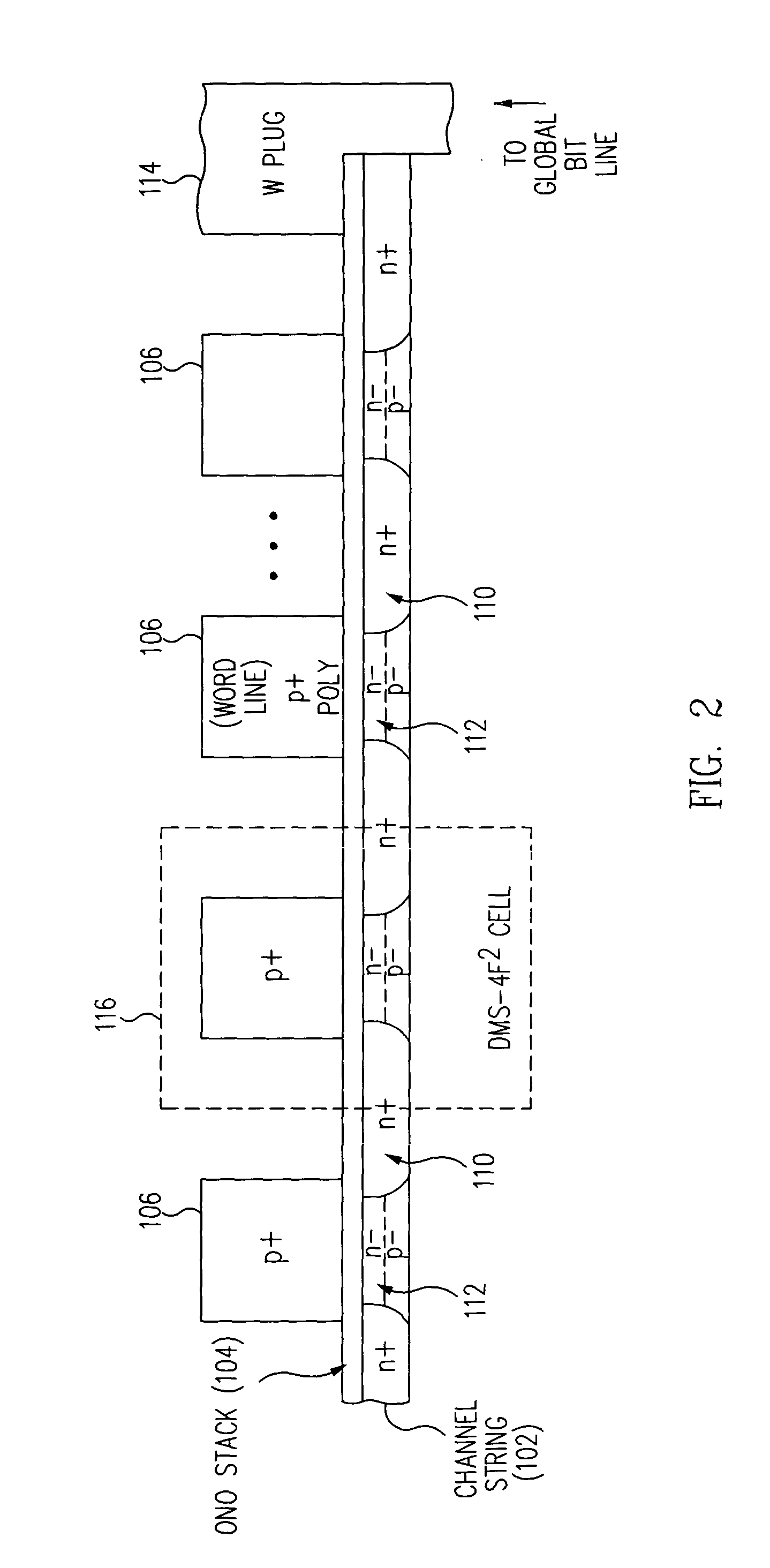
[0050] Referring now to FIG. 1, a three-dimensional view is shown conceptually depicting a portion of a two-level memory array 100 in accordance with the present invention. On level 1, a plurality of channel stripes (e.g., 102) is formed in a first direction. A stored charge dielectric layer 104, such as an oxide / nitride / oxide (ONO) stack, is formed at least on the top surface of the channel stripes 102. A plurality of gate stripes (e.g., 106) running in a second direction different than the first direction is formed on the stored charge dielectric layer 104. Preferably the gate stripes, also called word line stripes, run generally orthogonally to the channel stripes. A source / drain region (e.g., 110) is formed in the channel stripes in the exposed regions between the word line s...


PUM


Abstract

A three-dimensional flash memory array incorporates thin film transistors having a charge storage dielectric arranged in series-connected NAND strings to achieve a 4F<2 >memory cell layout. The memory array may be programmed and erased using only tunneling currents, and no leakage paths are formed through non-selected memory cells. Each NAND string includes two block select devices for respectively coupling one end of the NAND string to a global bit line, and the other end to a shared bias node. Pairs of NAND strings within a block share the same global bit line. The memory cells are preferably depletion mode SONOS devices, as are the block select devices. The memory cells may be programmed to a near depletion threshold voltage, and the block select devices are maintained in a programmed state having a near depletion mode threshold voltage. NAND strings on more than one layer may be connected to global bit lines on a single layer. By interleaving the NAND strings on each memory level and using two shared bias nodes per block, very little additional overhead is required for the switch devices at each end of the NAND strings. The NAND strings on different memory levels are preferably connected together by way of vertical stacked vias, each preferably connecting to more than one memory level. Each memory level may be produced with less than three masks per level.

Description

CROSS-REFERENCE TO RELATED APPLICATION(S)[0001] This application is related to co-pending U.S. application Ser. No. ______ ______ (Attorney Docket No. 023-0020) by Andrew J. Walker, et al, entitled "Method for Fabricating Programmable Memory Array Structures Incorporating Series-Connected Transistor Strings," filed on even date herewith, which application is hereby incorporated by reference in its entirety.[0002] 1. Field of the Invention[0003] The present invention relates to semiconductor integrated circuits containing memory arrays, and in preferred embodiments the invention particularly relates to monolithic three-dimensional memory arrays having series-connected memory cells.[0004] 2. Description of the Related Art[0005] Recent developments in semiconductor processing technologies and memory cell technologies have continued to increase the density achieved in integrated circuit memory arrays. For example, certain passive element memory cell arrays may be fabricated having word ...

Claims


Application Information

Patent Timeline
Patent Type & Authority Applications(United States)
IPC IPC(8): G11C11/56G11C16/04H01L21/8246H01L27/115
CPCG11C11/5621G11C16/0483H01L27/1159H01L27/11568H01L27/115H10B43/30H10B69/00H10B51/30
Inventor SCHEUERLEIN, ROY E.PETTI, CHRISTOPHERWALKER, ANDREW J.CHEN, EN-HSINGNALLAMOTHU, SUCHETAILKBAHAR, ALPERFASOLI, LUCAKOUZNETSOV, IGOR
Owner SANDISK TECH LLC
Why Eureka
Try Eureka