Method to Determine the Root Causes of Failure Patterns by Using Spatial Correlation of Tester Data

a technology of tester data and root cause, applied in the field of testing of semiconductor circuits, can solve problems such as short circuits or breakages in the circuitry of the integrated circuit chip arrangemen

Inactive Publication Date: 2008-12-04
IBM CORP
View PDF8 Cites 41 Cited by
  • Summary
  • Abstract
  • Description
  • Claims
  • Application Information

AI Technical Summary

Problems solved by technology

In one embodiment, the potential defects include breaks or short circuits within the circuitry of the integrated circuit chip arrangement.

Method used


Image

  • Method to Determine the Root Causes of Failure Patterns by Using Spatial Correlation of Tester Data
  • Method to Determine the Root Causes of Failure Patterns by Using Spatial Correlation of Tester Data
  • Method to Determine the Root Causes of Failure Patterns by Using Spatial Correlation of Tester Data

Examples


Embodiment Construction

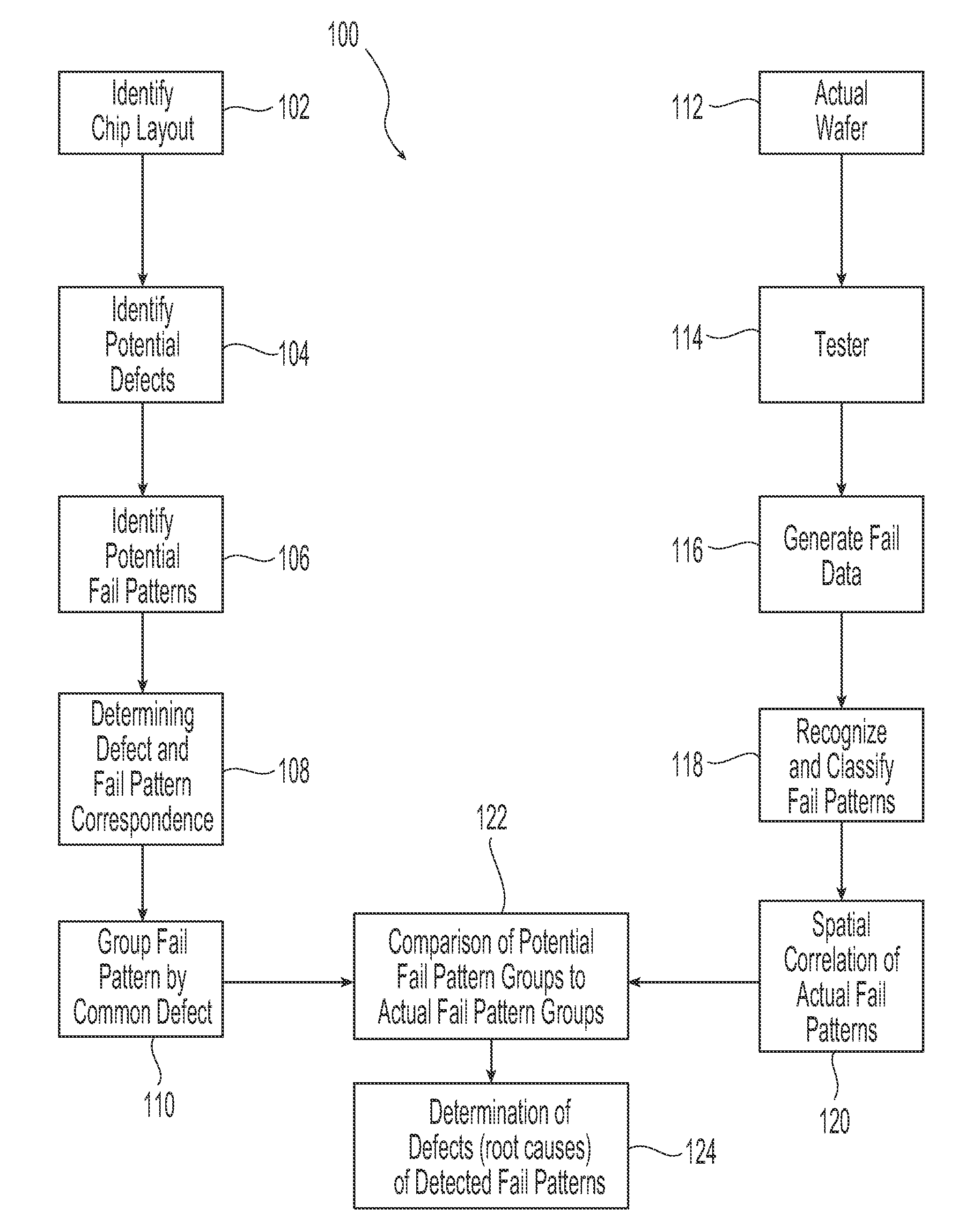
[0013]Systems and methods in accordance with the present invention correlate fail patterns in an integrated circuit chip or wafer with defect locations in that chip or wafer to identify the root cause of such fail patterns and to improve integrated circuit manufacturing yield. Referring initially to FIG. 1, an exemplary embodiment of a system 100 for the identification of defects that are the root cause of fail patterns in an integrated circuit chip in accordance with the present invention is illustrated. As illustrated, a known layout for each integrated circuit chip that is to be manufactured is identified 102. This layout is derived, for example, from a schematic used in the manufacture of the integrated circuit chip. The known layout for each integrated circuit chip is analyzed, and potential defects that can occur in the layout are identified 104. These manufacturing defects could cause open circuits and short circuits on the device and interconnect layers, for example on the s...


PUM


Abstract

A method for determining the root causes of fail patterns in integrated circuit chips is provide wherein a known integrated circuit chip layout is used to identify a plurality of potential defects and a plurality of potential fail patterns in the integrated circuit chip. Correlations between the potential defects and the potential fail patterns that result from those defects are identified. Based on this identification, the potential fail patterns are grouped by common potential defect. An actual integrated circuit chip that is manufactured in accordance with the test layout is tested for failure patterns. These failure patterns are then compared to the groupings of potential fail patterns. When a match is found, that is when a given group of fail patterns is found in the actual integrated circuit chip, then the potential defect associated with the potential fail patterns to which the actual fail patterns are matched is identified. This defect is the root cause of the failure pattern in the actual chip.

Description

FIELD OF THE INVENTION[0001]The present invention relates to testing of semiconductor circuits. More particularly, the present invention relates to a method and system of determining the root causes of fail patterns by utilizing the spatial correlation information of fail patterns and the layout information of the circuits.BACKGROUND OF THE INVENTION[0002]One of the main methods of improving circuit yield during the development or manufacturing of integrated circuits is to study the fail patterns uncovered by a tester used to test a given integrated circuit. If fail patterns could be used to disclose important information about their root causes or the nature of the defects, corrective actions could then be taken to improve the yield, based on the knowledge of such defects gained from such analysis, either from the process side or the design side.[0003]Existing methods for analyzing semiconductor fail patterns are developed from the memory bit fail maps. Unlike logic circuits, memor...

Claims


Application Information

Patent Timeline
Patent Type & Authority Applications(United States)
IPC IPC(8): G06F17/50
CPCG01R31/2894G01R31/31718G01R31/318314G11C29/10G11C29/56G11C29/56008
Inventor CHEN, HOWARDHAWKINS, KATHERINE V.HENG, FOOK-LUENHSU, LOUISOUYANG, XU
Owner IBM CORP
Why Eureka
Try Eureka