Optical device and method for fabricating the same, camera module using optical device, and electronic equipment mounting camera module

a technology of optical devices and optical components, applied in the direction of solid-state devices, color television, television systems, etc., can solve the problems of the functionality of the microlens, and achieve the effects of reducing the stress on the microlens, preventing the inhibition of the functionality of the microlens and the like, and reducing the thickness

Active Publication Date: 2008-12-11
GK BRIDGE 1
View PDF1 Cites 46 Cited by
  • Summary
  • Abstract
  • Description
  • Claims
  • Application Information

AI Technical Summary

Benefits of technology

The present invention provides an optical device with a small size and low cost. The device includes a light receiving element chip with an external connection terminal on the back surface, which allows for a sufficient thickness of the planarization film. A transparent protective film is formed on the planarization film to reduce stress to the microlens and prevent its functionality from being affected by adhering particles. Additionally, the device does not require a conventional ceramic package, making it even more cost-effective.

Problems solved by technology

The technical problem addressed in this patent text is the need to enhance the sensitivity of solid-state imaging devices without compromising the reliability and thickness of the device. The conventional methods for increasing the aperture ratio of the microlens include increasing the area of the photodiode, but this method has limitations in terms of pattern design and cost. Other methods include adding a microlens cover film or a protective layer with a higher mechanical strength, but these methods have limitations in terms of cost and thickness. The patent text proposes several new methods for increasing the aperture ratio of the microlens, including increasing the area of the microlens, adding a microlens cover film, and protecting the microlens with a cover glass. These methods need to be further developed and tested in order to improve their effectiveness.

Method used


Image

  • Optical device and method for fabricating the same, camera module using optical device, and electronic equipment mounting camera module
  • Optical device and method for fabricating the same, camera module using optical device, and electronic equipment mounting camera module
  • Optical device and method for fabricating the same, camera module using optical device, and electronic equipment mounting camera module

Examples


first embodiment

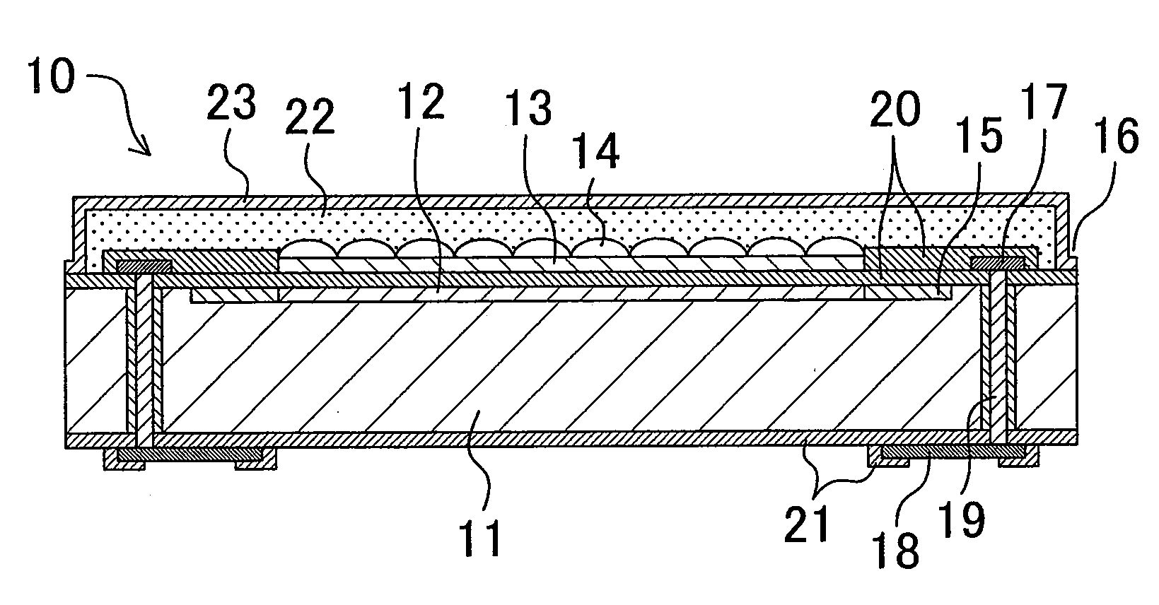
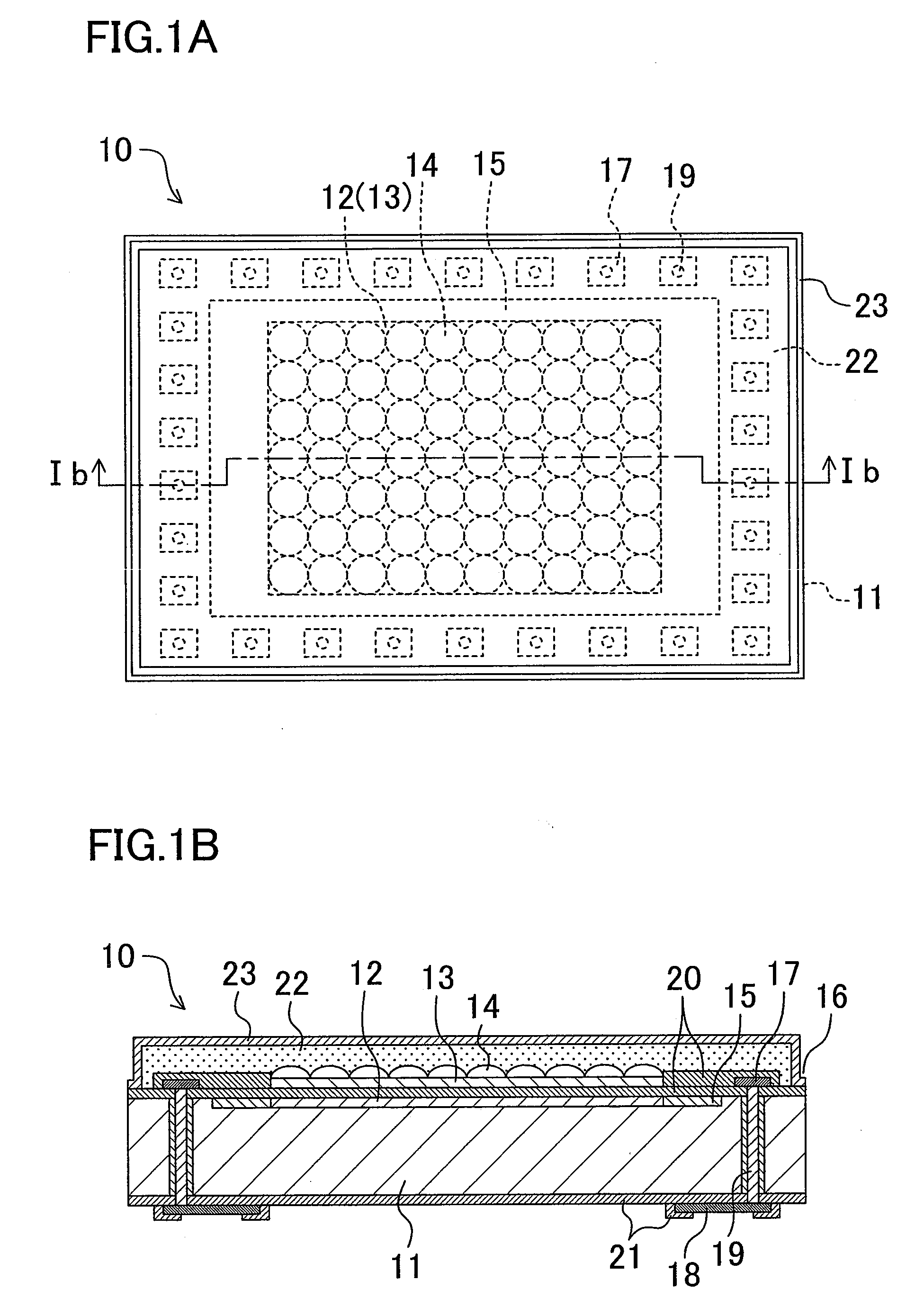
[0042]FIGS. 1A and 1B are views showing the structure of an optical device according to a first embodiment of the present invention. FIG. 1A is a plan view thereof, and FIG. 1B is a sectional view taken along the line Ib-Ib. In the first embodiment, as the optical device, a solid-state imaging device employed in a digital camera and the like will be described as one example. In the following description, the optical device is represented as a solid-state imaging device 10.

[0043]The solid-state imaging device 10 according to the first embodiment is mainly composed of a light receiving element chip, microlenses 14, a planarization film 22, and a transparent protective film 23. The light receiving element chip includes an active region 12, a circuit region 15, a penetrating conductor 19, and an external connection terminal 18. The active region 12 is formed on the principal plane of a substrate 11, and made by arranging a plurality of light receiving pixels. The circuit region 15 is di...

second embodiment

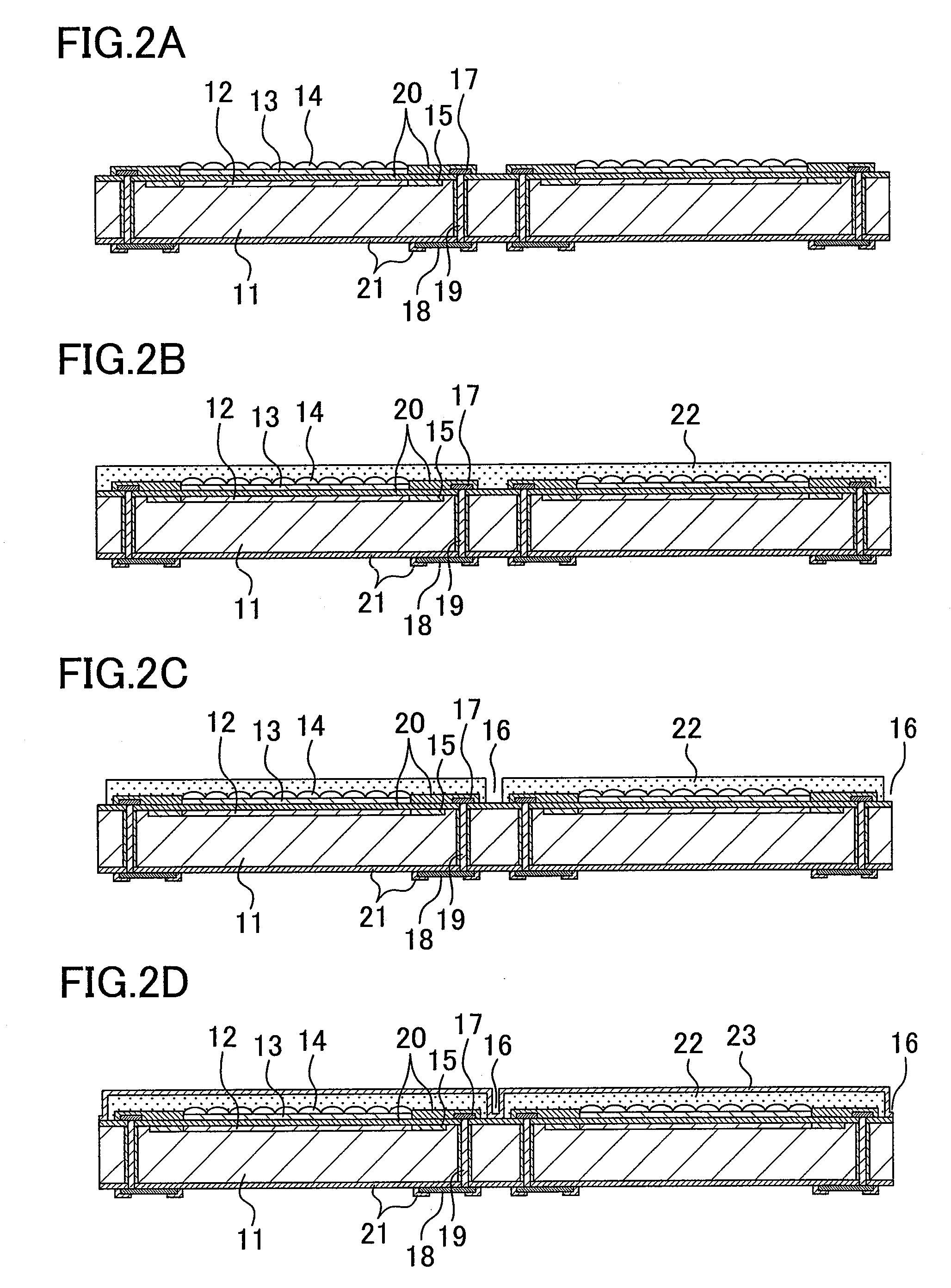
[0080]FIGS. 6A and 6B are views showing the structure of an optical device according to a second embodiment of the present invention. FIG. 6A is a plan view thereof, and FIG. 6B is a sectional view taken along the line VIb-VIb. In the second embodiment, as the optical device, a solid-state imaging device employed in a digital camera and the like will be described as one example. In the following description, the optical device is represented as a solid-state imaging device 80.

[0081]In the solid-state imaging device 80 according to the second embodiment, a basic structure, materials, and the like are identical to the above-described solid-state imaging device 10 according to the first embodiment, and hence their description is not repeated.

[0082]Referring to FIGS. 6A and 6B, the solid-state imaging device 80 according to the second embodiment is characterized in that the planarization film 22 and the transparent protective film 23 are formed over the entire surface of the principal p...


PUM


Abstract

An optical device includes a light receiving element chip having: an active region formed on a principal plane of a substrate and made by arranging a plurality of light receiving pixels; a circuit region disposed around an outer circumference of the active region; a penetrating conductor provided to penetrate the substrate in the thickness direction of the substrate; and an external connection terminal provided on a back surface of the substrate facing the principal plane thereof and connected to the penetrating conductor. The optical device further includes a microlens, a planarization film, and a transparent protective film formed on the planarization film.

Description


Claims


Application Information

Patent Timeline
Owner GK BRIDGE 1
Why Eureka
Try Eureka