Multi-layered ceramic electronic component

a ceramic electronic component and multi-layer technology, applied in the direction of fixed capacitor details, capacitors, fixed capacitors, etc., can solve the problems of minute gaps between the ends of the internal electrode and the ceramic layer during firing, and the level difference between the internal electrode and the ceramic layer is not uniform, so as to achieve high moisture resistance. the effect of reliabl

Active Publication Date: 2008-12-11
MURATA MFG CO LTD
View PDF12 Cites 65 Cited by
  • Summary
  • Abstract
  • Description
  • Claims
  • Application Information

AI Technical Summary

Benefits of technology

[0013]To overcome the problems described above, preferred embodiments of the present invention provide a multi-layered ceramic electronic component having highly reliable moisture resistance even when the component has a small size.

Problems solved by technology

The internal electrodes are arranged at inner locations of the ceramic layers and away from peripheries of the ceramic layers, thus causing differences in the level between the internal electrodes and the ceramic layers.
An increase in the number of stacked ceramic layers is likely to cause structural defects, such as delamination, due to such level differences.
However, minute gaps are formed between ends of the internal electrodes and the ceramic layers during firing due to differences in shrinkage behavior during sintering between the internal electrodes and the ceramic layers.
Thus, the chip has poor resistance to moisture.
Even in the method disclosed in Japanese Unexamined Patent Application Publication No. 2004-96010, however, it is very difficult to completely match the shrinkage behavior during sintering of the ceramic to that of the internal electrodes, and thus, this solution to the problem of poor moisture resistance due to the gaps is not satisfactory.
Thereby, gaps located near side surfaces are excessively sintered, which is likely to cause problems of structural defects and a reduction in the strength of the main body of a capacitor.
Thus, currently it is difficult to ensure sufficiently reliable moisture resistance for a multi-layered chip.

Method used


Image

  • Multi-layered ceramic electronic component
  • Multi-layered ceramic electronic component
  • Multi-layered ceramic electronic component

Examples


first preferred embodiment

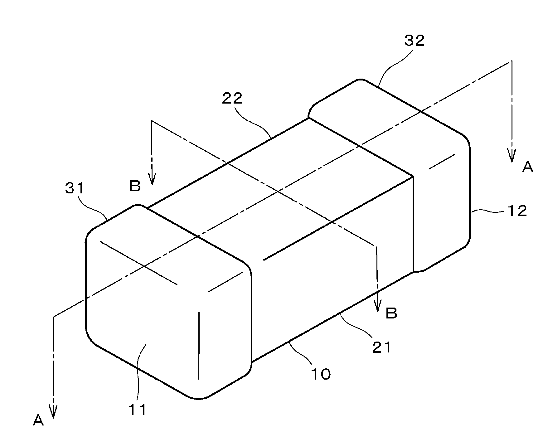
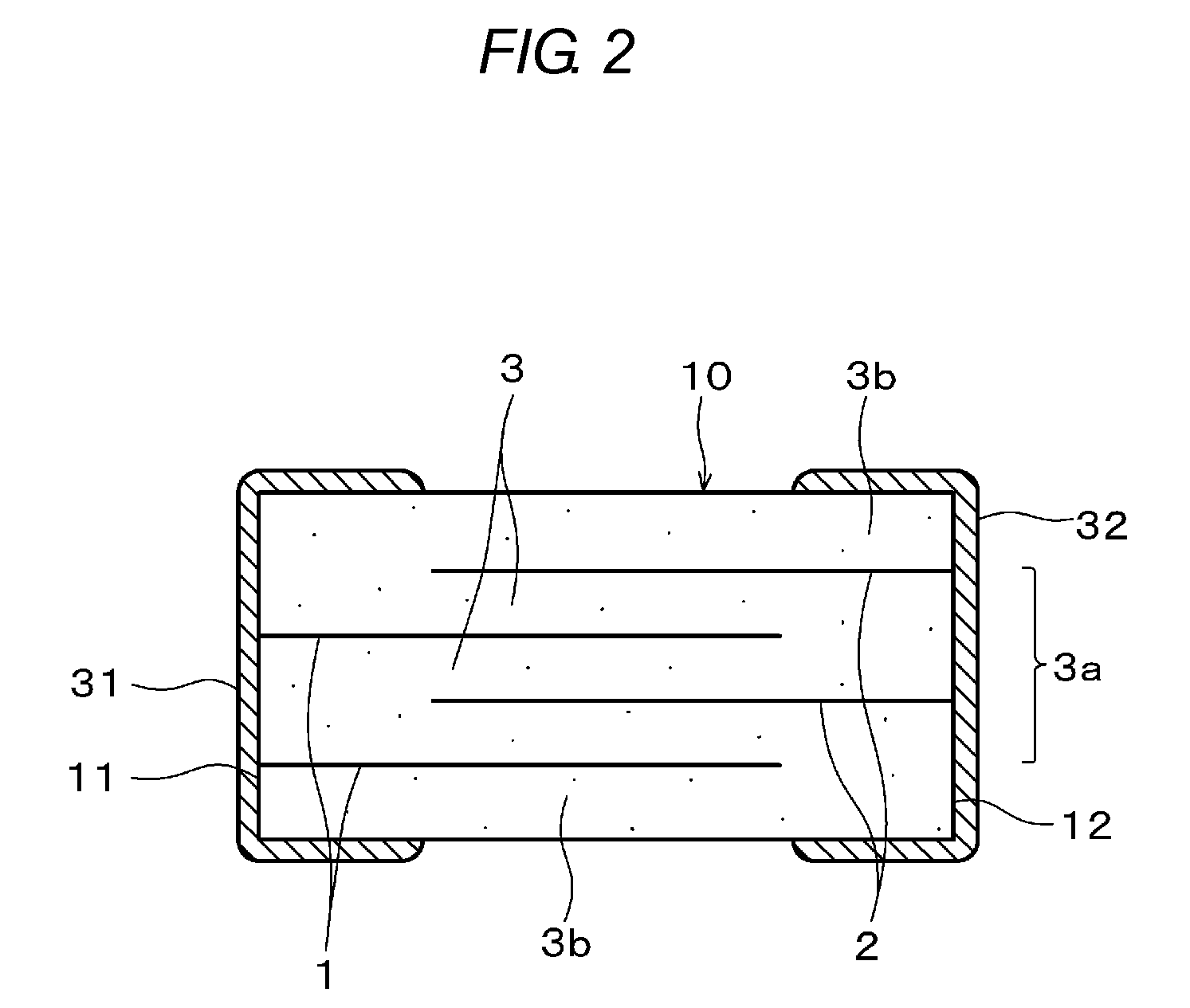
[0045]FIG. 1 is a perspective view illustrating a multi-layered ceramic electronic component (in this preferred embodiment, a multi-layered ceramic capacitor) according to a preferred embodiment of the present invention. FIG. 2 is a cross-sectional view taken along line A-A in FIG. 1. FIG. 3 is a cross-sectional view taken along line B-B in FIG. 1. FIG. 4 is an explanatory drawing illustrating the structure of a multi-layered ceramic capacitor according to a first preferred embodiment of the present invention.

[0046]As shown in FIGS. 1 to 4, a multi-layered ceramic capacitor according to the first preferred embodiment includes a sintered ceramic body 10 in which a plurality of ceramic layers 3 are stacked, first internal electrodes 1 and second internal electrodes 2 alternately arranged in the sintered ceramic body, one end of each of the first internal electrodes 1 extending to a first end surface 11 of the sintered ceramic body 10, and one end of each of the second internal electro...

second preferred embodiment

[0081]FIG. 7 is a fragmentary cross-sectional view of a multi-layered ceramic electronic component (in this preferred embodiment, a multi-layered ceramic capacitor) according to another preferred embodiment of the present invention. FIG. 7 is a view taken along line B-B in FIG. 1 according to the first preferred embodiment. FIG. 8 is an explanatory drawing of a multi-layered ceramic capacitor according to the second preferred embodiment of the present invention.

[0082]In the multi-layered ceramic capacitor according to the second preferred embodiment as shown in FIGS. 7 and 8, the side gap portions GS are Mg-rich regions MR, and side gap vertical extensions 13b that vertically extend from the side gap portions GS, in the ceramic layers located outside the outermost internal electrodes (the external layers 3b) are also Mg-rich regions MR.

[0083]In the multi-layered ceramic capacitor according to the second preferred embodiment, each of the Mg-rich regions MR has a concentration gradien...

third preferred embodiment

[0095]FIG. 9 is a fragmentary cross-sectional view of a multi-layered ceramic electronic component (in this preferred embodiment, a multi-layered ceramic capacitor) according to another preferred embodiment of the present invention. FIG. 9 is a view taken along line B-B in FIG. 1 according to the first preferred embodiment. FIG. 10 is an explanatory drawing of a multi-layered ceramic capacitor according to the third preferred embodiment of the present invention.

[0096]In the multi-layered ceramic capacitor according to the third preferred embodiment as shown in FIGS. 9 and 10, the side gap portions GS are Mg-rich regions MR, and side gap vertical extensions 13b that vertically extend from the side gap portions GS, in the ceramic layers located outside the outermost internal electrodes (the external layers 3b) are also Mg-rich regions MR.

[0097]As shown in FIG. 10, no Mg-rich region is formed in the end gap portions GE.

[0098]The multi-layered ceramic capacitor according to the third pr...


PUM

PropertyMeasurementUnit
temperatureaaaaaaaaaa
thicknessaaaaaaaaaa

Abstract

In a sintered ceramic body including side gap portions arranged between sides of first and second internal electrodes and first and second side surfaces of the sintered ceramic body and between sides of the effective layer portion and the first and second side surfaces of the sintered ceramic body, regions of the side gap portions at least adjacent to the first and second internal electrodes are Mg-rich regions each having a Mg concentration greater than that of the effective layer portion.

Description

BACKGROUND OF THE INVENTION[0001]1. Field of the Invention[0002]The present invention relates to ceramic electronic components, and more specifically, it relates to a multi-layered ceramic electronic component including ceramic layers and internal electrodes to generate capacitance.[0003]2. Description of the Related Art[0004]In recent years, as electronic apparatuses, such as mobile phones and portable music players, are being downsized, electronic components to be mounted thereon have been downsized. For example, in multi-layered chip ceramic electronic components typified by multi-layered chip ceramic capacitors, in order to reduce the chip size while maintaining desired properties, the thickness of their ceramic layers has been reduced.[0005]With the reduction in the thickness of the ceramic layers, there is a tendency to stack a greater number of thin ceramic layers. Usually, a multi-layered ceramic electronic component includes ceramic layers and internal electrodes that are a...

Claims


Application Information

Patent Timeline
Patent Type & Authority Applications(United States)
IPC IPC(8): H01G4/06
CPCH01G4/012H01G4/232H01G4/30
Inventor SUZUKI, KOJI
Owner MURATA MFG CO LTD
Why Eureka
Try Eureka