Wavelength converter, light-emitting device using same, and production method for wavelength converter
a technology of light-emitting devices and wavelength converters, applied in the field of wavelength converters, can solve the problems of large installation space, large production cost, and disadvantageous increase in production costs of amber light-emitting led chips, and achieve the effects of low temperature dependence of emission color, excellent luminescent efficiency, and small specific surface area
- Summary
- Abstract
- Description
- Claims
- Application Information
AI Technical Summary
Benefits of technology
Problems solved by technology
Method used
Image
Examples
example 1
(Wavelength Converter)
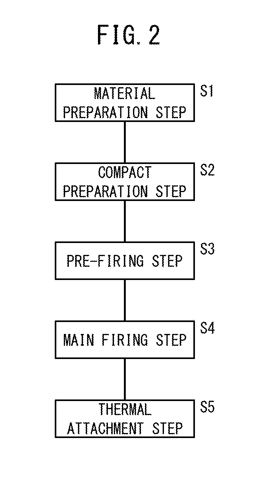
[0081]A light transmissive substrate 20 having a purity of 99.9%, a relative density of 99.5% or more (measured by the Archimedes method), an average grain diameter of 20 μm, an outer size of 100×100 mm, and a thickness of 0.5 mm was obtained using a gel casting method described in Japanese Laid-Open Patent Publication No. 2001-335371.
[0082]Specifically, a high-purity alumina powder having a purity of 99.99% or more, a BET surface area of 9 to 15 m2 / g, and a tap density of 0.9 to 1.0 g / cm3 was doped with auxiliary agents of 300 ppm of an MgO powder, 300 ppm of a ZrO2 powder, and 50 ppm of a Y2O3 powder. The obtained material powder was shaped by the gel casting method.
[0083]The material powder and a dispersing agent were added to and dispersed in a dispersion medium at 20° C., a gelling agent was added thereto and dispersed therein, and a reaction catalyst was further added thereto to obtain slurry. The slurry was cast into a mold and left for 2 hours to conver...
example 2
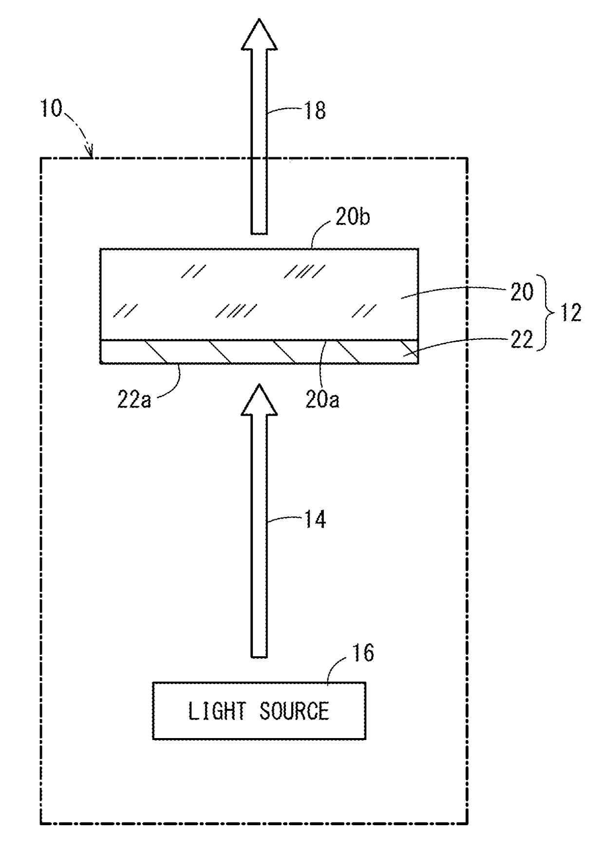
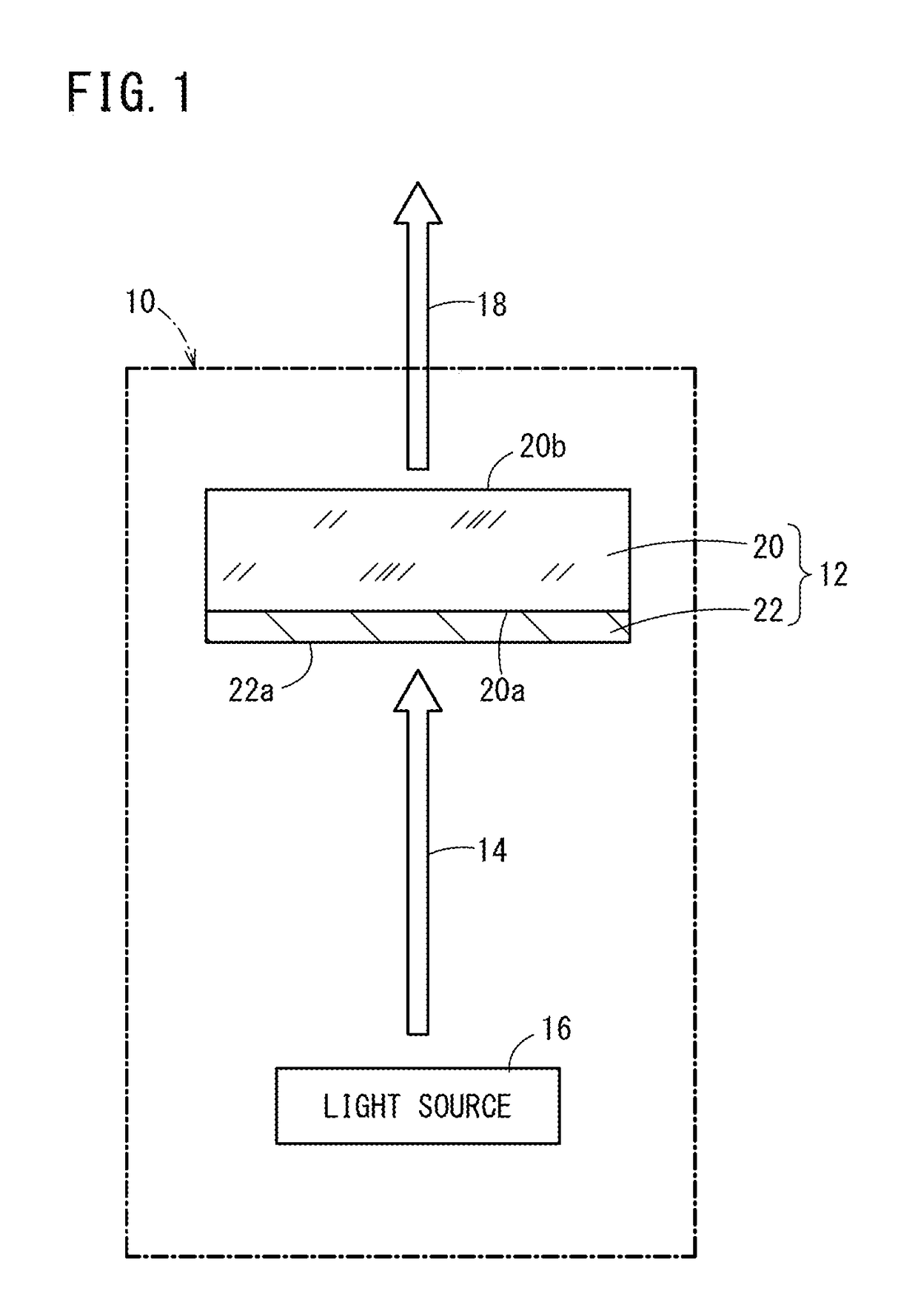
[0088]The wavelength converter 12 of Example 2 was produced in the same manner as Example 1 except that the thin film 22 had a thickness of 210 μm. The effective thickness of the phosphor in the thin film 22 was 60 vol %×210 μm=12600 vol %·μm. The above light source 16 described in Example 1 was used also in Example 2.
example 3
[0089]The wavelength converter 12 of Example 3 was produced in the same manner as Example 1 except that the volume ratio of phosphor / glass was 90 vol % / 10 vol %, and the thin film 22 had a thickness of 60 μm. The effective thickness of the phosphor in the thin film 22 was 90 vol %×60 μm=5400 vol %·μm. The above light source 16 described in Example 1 was used also in Example 3.
PUM
| Property | Measurement | Unit |
|---|---|---|
| average grain diameter | aaaaa | aaaaa |
| softening point | aaaaa | aaaaa |
| volume ratio | aaaaa | aaaaa |
Abstract
Description
Claims
Application Information


