Microstructure transfer medium and application thereof

a microstructure and transfer medium technology, applied in the direction of electric/magnetic/electromagnetic heating, instruments, lighting and heating apparatus, etc., can solve the problems defects at the sharp vertex or mold releasing imperfections, etc., and achieve the effect of low cost of the microstructure transfer medium

Inactive Publication Date: 2008-12-11
LENTICS CORP
View PDF0 Cites 23 Cited by
  • Summary
  • Abstract
  • Description
  • Claims
  • Application Information

AI Technical Summary

Benefits of technology

[0011]In accordance with the present invention, a microstructure transfer medium is provided to fabricate a microstructure film. The microstructure transfer medium comprises a substrate and a release layer formed on the substrate. The release layer has microstructures thereon. Preferably, the surface energy of the release layer is lower than 30 dyne/cm. More preferably, the surface energy of the release layer is lower than 25 dyne/cm. T

Problems solved by technology

Thus, during fabricating a microstructure film, the problems of defects at the sharp vertex or mold rel

Method used


Image

  • Microstructure transfer medium and application thereof
  • Microstructure transfer medium and application thereof

Examples


Embodiment Construction

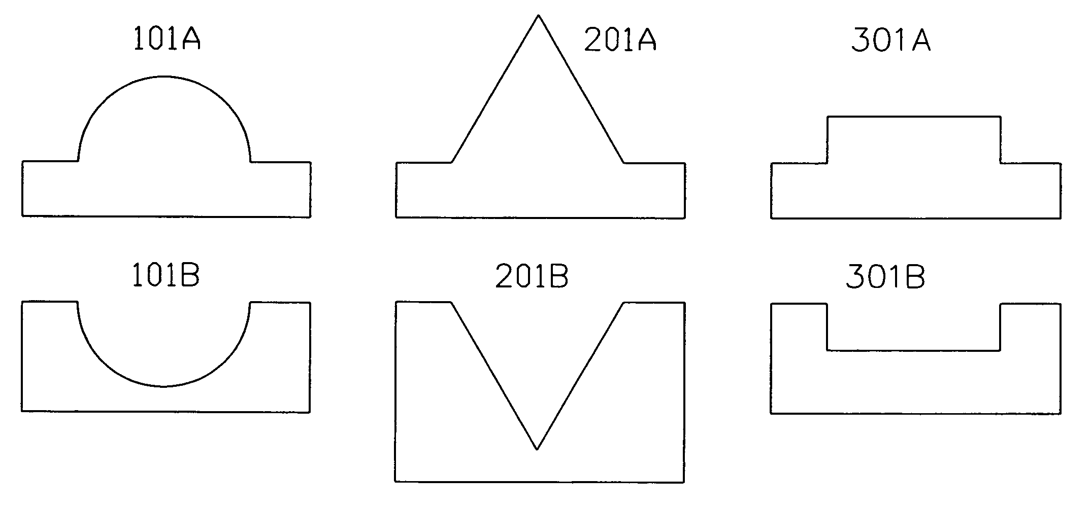
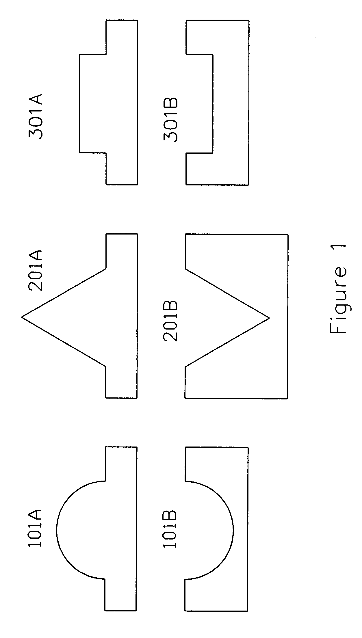
[0019]What is probed into the invention is a microstructure transfer medium. Detail descriptions of the structure and elements will be provided in the following in order to make the invention thoroughly understood. Obviously, the application of the invention is not confined to specific details familiar to those who are skilled in the art. On the other hand, the common structures and elements that are known to everyone are not described in details to avoid unnecessary limits of the invention. Some preferred embodiments of the present invention will now be described in greater detail in the following. However, it should be recognized that the present invention can be practiced in a wide range of other embodiments besides those explicitly described, that is, this invention can also be applied extensively to other embodiments, and the scope of the present invention is expressly not limited except as specified in the accompanying claims.

[0020]The microstructure transfer medium according ...


PUM

PropertyMeasurementUnit
Surface energyaaaaaaaaaa
Adhesion strengthaaaaaaaaaa
Flexibilityaaaaaaaaaa

Abstract

The present invention discloses a microstructure transfer medium and application thereof to produce various microstructures on a film, glass substrate, plastic substrate, etc. for utilization in a variety of optical films of a backlight module, light guide plates, color enhancement film for liquid crystal displays, various patterned nanoimprint for semiconductor or flat panel display processes, and Fresnel lens. Furthermore, the microstructure transfer medium according to the present invention can be applied in producing microstructures on a non-planar surface. The microstructure transfer medium according to the present invention comprises a substrate and a release layer formed on the substrate wherein the release layer has microstructures thereon. Preferably, the surface energy of the release layer is lower than 30 dyne/cm.

Description

BACKGROUND OF THE INVENTION[0001]1. Field of the Invention[0002]The present invention is generally related to a microstructure transfer medium and application thereof, and more particularly to a microstructure transfer medium applied in a variety of optical films of a backlight module, light guide plates, color enhancement film for liquid crystal displays, various patterned nanoimprint for semiconductor or flat panel display processes, and Fresnel lens.[0003]2. Description of the Prior Art[0004]Microstructure films have been extensively applied in various areas, such as lighting, advertising lighting boxes, backlights, and displays.[0005]In backlight modules, the optical members with microstructures, such as brightness enhancement film and light guide plate, are usually made by firstly preparing a metallic mold with microstructures and then setting the resin in the metallic mold via an ultraviolet curing or injection molding method.[0006]However, for example of fabricating brightnes...

Claims


Application Information

Patent Timeline
IPC IPC(8): F21V8/00F21V5/02F21V5/04
CPCB29C33/3842B29C33/424B29D11/00663G02B3/08G02B6/0036G02B6/0065Y10T428/31909
Inventor CHIANG, WHE YIPONG, TA CHING
Owner LENTICS CORP
Why Eureka
Try Eureka