Conformal EMI shielding with enhanced reliability

a technology of emi shielding and reliability, applied in the field of semiconductor device packaging, can solve the problems of increasing the cost and complexity of the packaging process, not providing protection against interference caused by modules within the board or system,

Inactive Publication Date: 2008-12-25
FREESCALE SEMICON INC
View PDF14 Cites 26 Cited by
  • Summary
  • Abstract
  • Description
  • Claims
  • Application Information

AI Technical Summary

Problems solved by technology

Conventional approaches for shielding against EMI have used board or system level EMI shielding techniques, though this does not provide protection against interference caused by modules within the board or s

Method used


Image

  • Conformal EMI shielding with enhanced reliability
  • Conformal EMI shielding with enhanced reliability
  • Conformal EMI shielding with enhanced reliability

Examples


Embodiment Construction

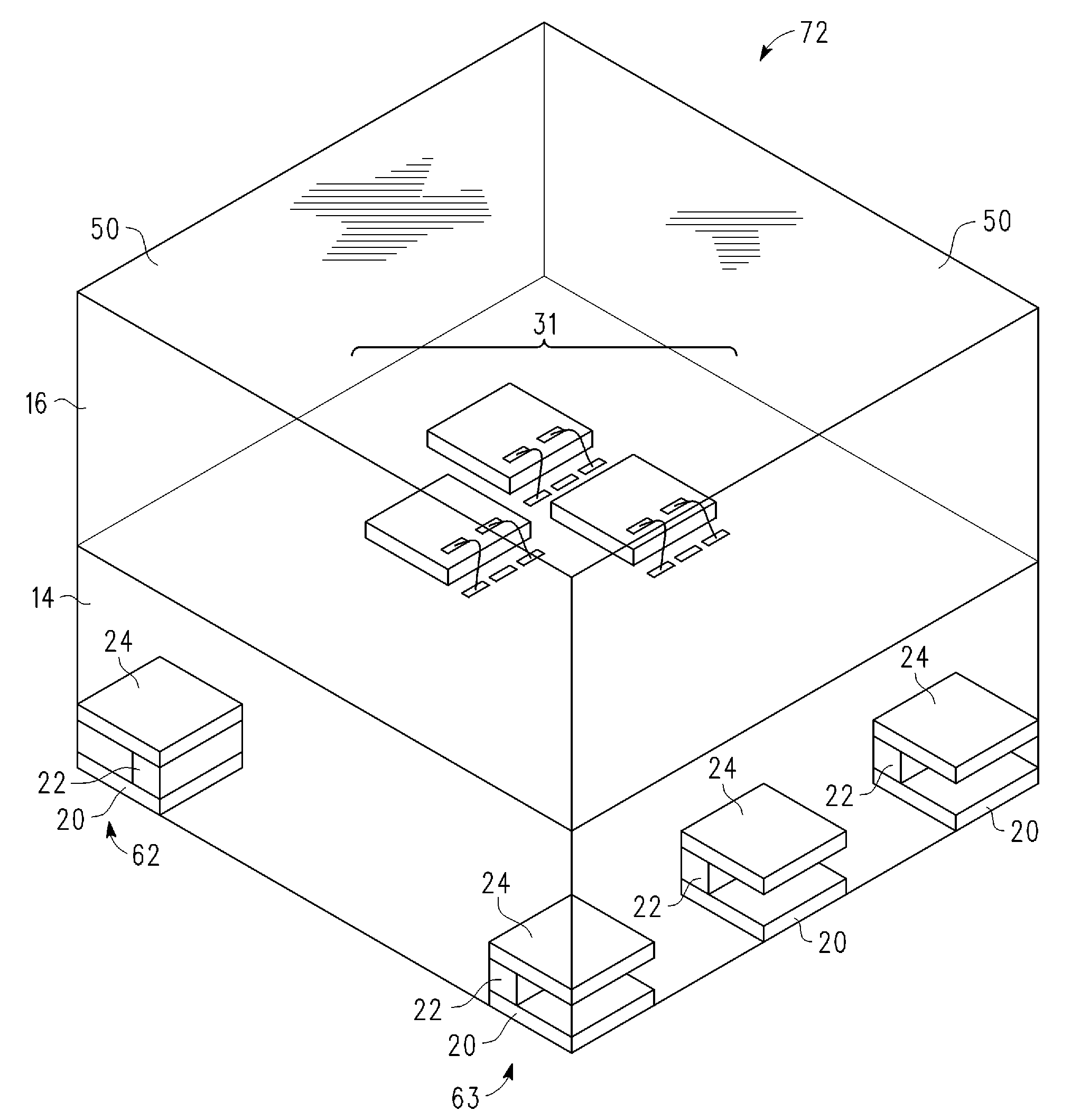
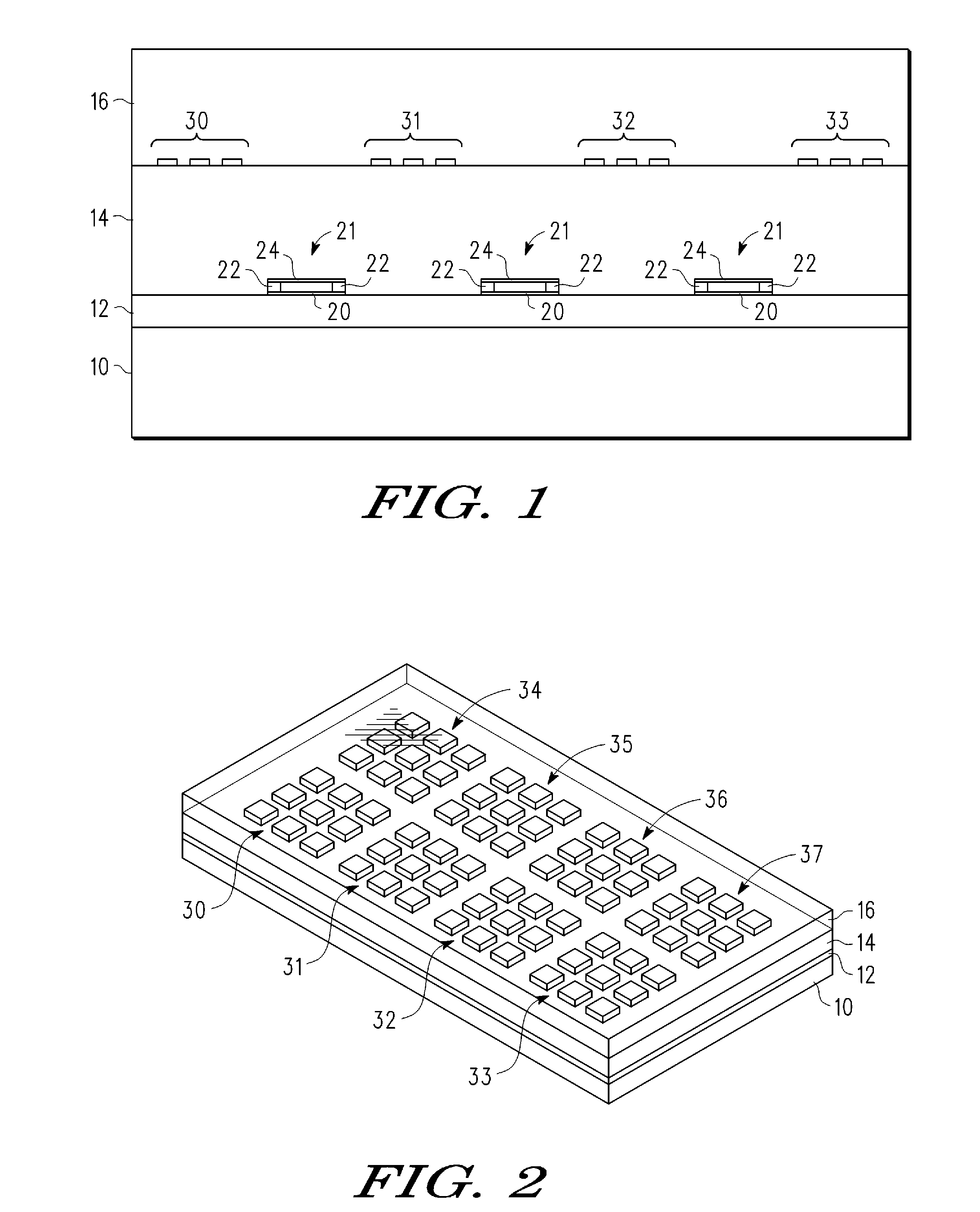
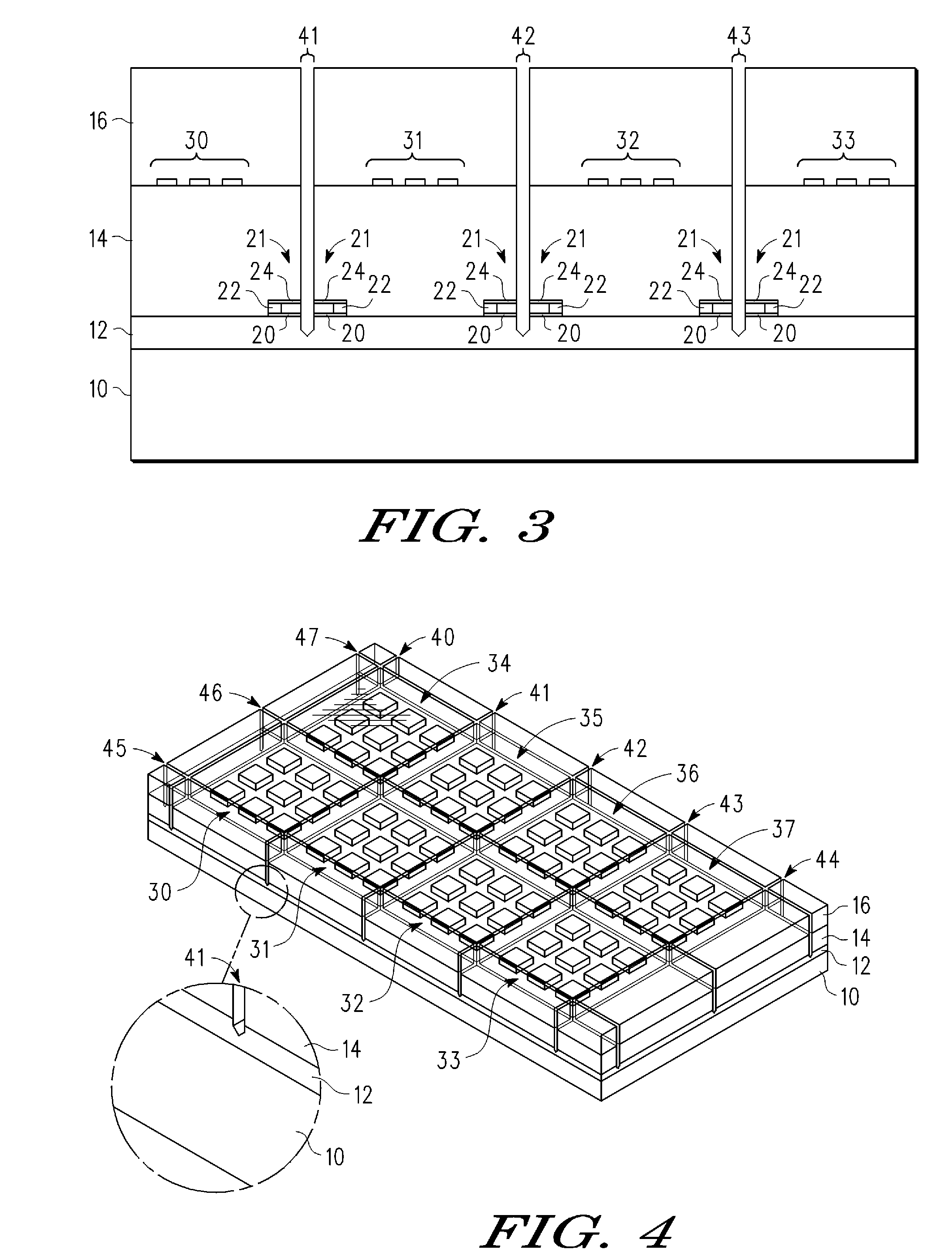
[0016]A method and apparatus are described for fabricating a shielded encapsulated semiconductor device or devices. As a preliminary step, a package panel is assembled by mounting a plurality of devices onto a circuit substrate and then encapsulating the plurality of devices with a molding compound. The package panel is then mounted on a process carrier by using a removable attachment device, such as a thick double-sided tape or chemical attachment layer, to adhere the package panel to the process carrier. Once mounted, the package panel is singulated or cut using any desired saw or cutting process, such as laser cutting. By cutting through the molding compound and circuit substrate and into the attachment device, grooves are formed between the individual chip modules all the way down into the attachment device. After the grooves are formed, a shielding material cover layer is conformally formed over the molding compound and in the grooves (e.g., by sputtering, spraying, etc.), ther...


PUM


Abstract

An electromagnetic interference (EMI) and/or electromagnetic radiation shield is formed on a plurality of encapsulated modules by attaching a molded package panel to a process carrier (10) using a double side adhesive tape (12) before singulating the individual modules without separating them from the double side adhesive tape. By forming a conductive layer (50) over a mold encapsulant (16) and on the sidewalls of grooves (40-47) that are cut through the mold encapsulant (16) and underlying circuit substrate (14), the conductive layer (50) may be electrically coupled to one or more conductive connection pads (61-66) by virtue of the placement of the conductive connection pads at the periphery or side of the circuit substrate (14).

Description

BACKGROUND OF THE INVENTION[0001]1. Field of the Invention[0002]The present invention is directed in general to the field of semiconductor devices. In one aspect, the present invention relates to semiconductor packaging devices which are shielded to protect against electromagnetic interference (EMI).[0003]2. Description of the Related Art[0004]Semiconductor devices need to be protected from electromagnetic interference (EMI) which is the undesired electrical signals, or noise, in electronic system circuitry caused by the unintentional coupling of electromagnetic field energy from other circuitry, such as wires, printed circuit board conductors, connector elements, connector pins, cables, and the like. For example, multiple chip modules (MCM) are semiconductor devices having a plurality of discrete microelectronic devices (e.g., a processor unit, memory unit, related logic units, resistors, capacitors, inductors, and the like) that are connected together on a single MCM substrate. Co...

Claims


Application Information

Patent Timeline
IPC IPC(8): H01L23/552H01L21/56
CPCH01L21/568H01L23/3121H01L23/552H01L25/0652H01L2924/09701H01L2924/19041H01L2924/3025H01L24/97H01L25/0655H01L2224/48227H01L2224/97H01L2224/85H01L2924/01029H01L2224/85005H01L2924/181H01L2224/05553H01L2924/00
Inventor TANG, JINBANGLIN, JONG-KAI
Owner FREESCALE SEMICON INC
Why Eureka
Try Eureka