Display Panel, Electro-Optical Device, and Methods for Fabricating the Same

a technology of electrooptical devices and display panels, applied in static indicating devices, non-linear optics, instruments, etc., can solve the problems of poor contrast ratio, more power consumption of backlight modules, unclear images, etc., to improve the efficiency of liquid crystals, improve the dark-state light leakage, and improve the contrast ratio

Active Publication Date: 2008-12-25
AU OPTRONICS CORP
View PDF7 Cites 8 Cited by
  • Summary
  • Abstract
  • Description
  • Claims
  • Application Information

AI Technical Summary

Benefits of technology

[0015]By using the configuration of scan lines and common lines to change the electric field distribution of a display panel, the display panel and the electro-optical device of this invention achieves a regular arrangement of liquid crystals within the display panel, which may enhance the efficiency of the liquid crystals and improve the dark-state light leakage, thus improving the contrast ratio.

Problems solved by technology

The brighter the LCD display, the more power the backlight module consumes.
Moreover, under bright environments, the displayed images are prone to interference from ambient light, which may render the images unclear.
In contrast, a reflective type LCD displays an image by reflecting ambient light, which, may be consumer less power, but exhibits a poor contrast ratio, a degraded color saturation, and cannot display images clearly in dark conditions.
For example, in a low temperature polysilicon (LTPS) technology, a scan line is exposed to an 11 V potential when TFT is switched off in micro-second (μsec), while the common line stays at 0 V A higher electric potential difference between the common line and the scan line tends to cause uneven an electric field distribution on both sides, which may result in different tilt degrees of the liquid crystals and an irregular arrangement of liquid crystals near the scan line, thus leading to a dark-state leakage and degraded contrast ratio.
In summary, the existing TFT-LCDs with the MVA design exhibit an irregular arrangement of liquid crystal molecules when powered on, which may result in a low efficiency of liquid crystal molecules and affect the brightness distribution.
Furthermore, there is a dark-state light leakage and degraded contrast ratio, thereby adversely affecting the image displaying quality.

Method used


Image

  • Display Panel, Electro-Optical Device, and Methods for Fabricating the Same
  • Display Panel, Electro-Optical Device, and Methods for Fabricating the Same
  • Display Panel, Electro-Optical Device, and Methods for Fabricating the Same

Examples


first embodiment

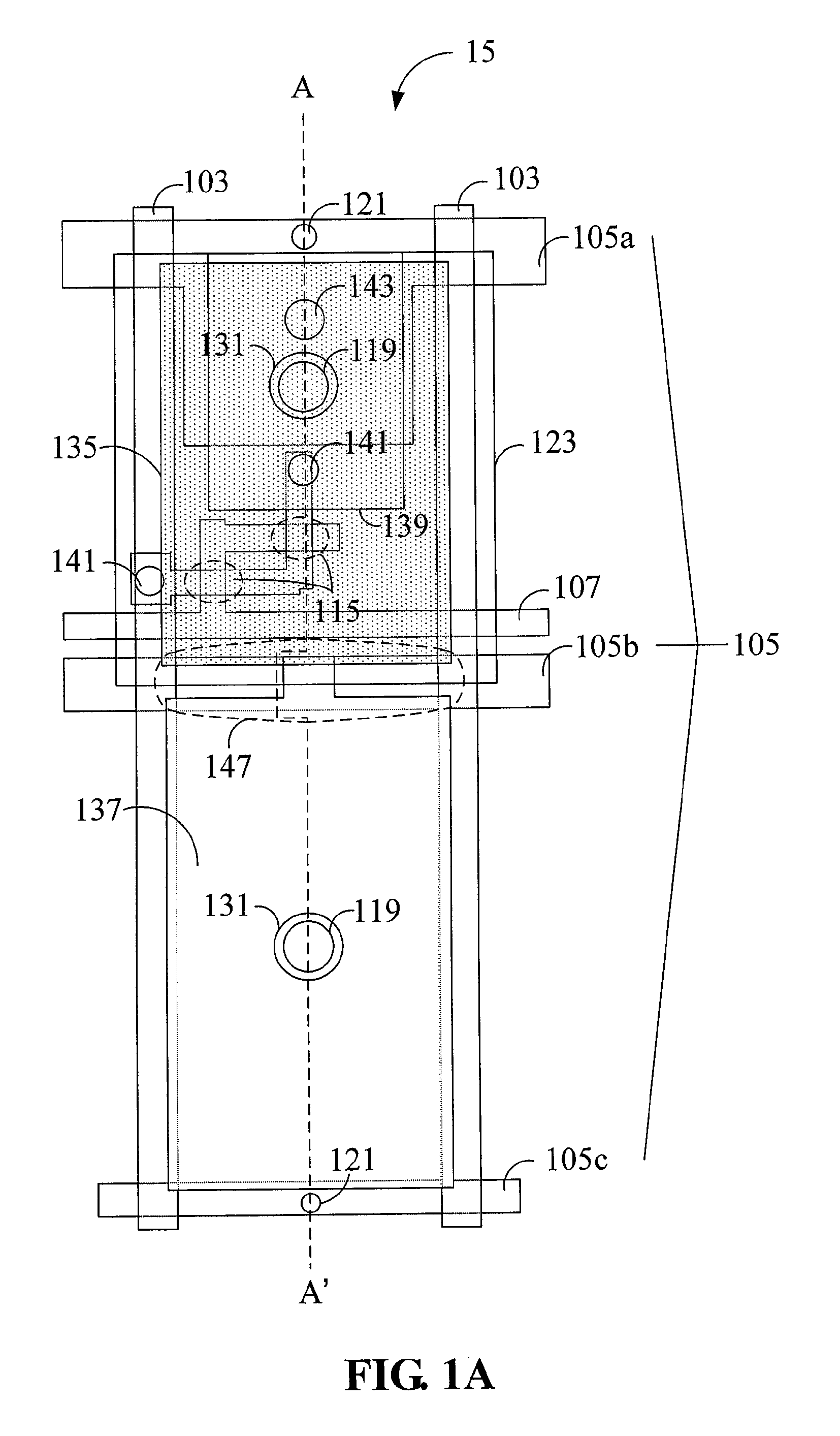
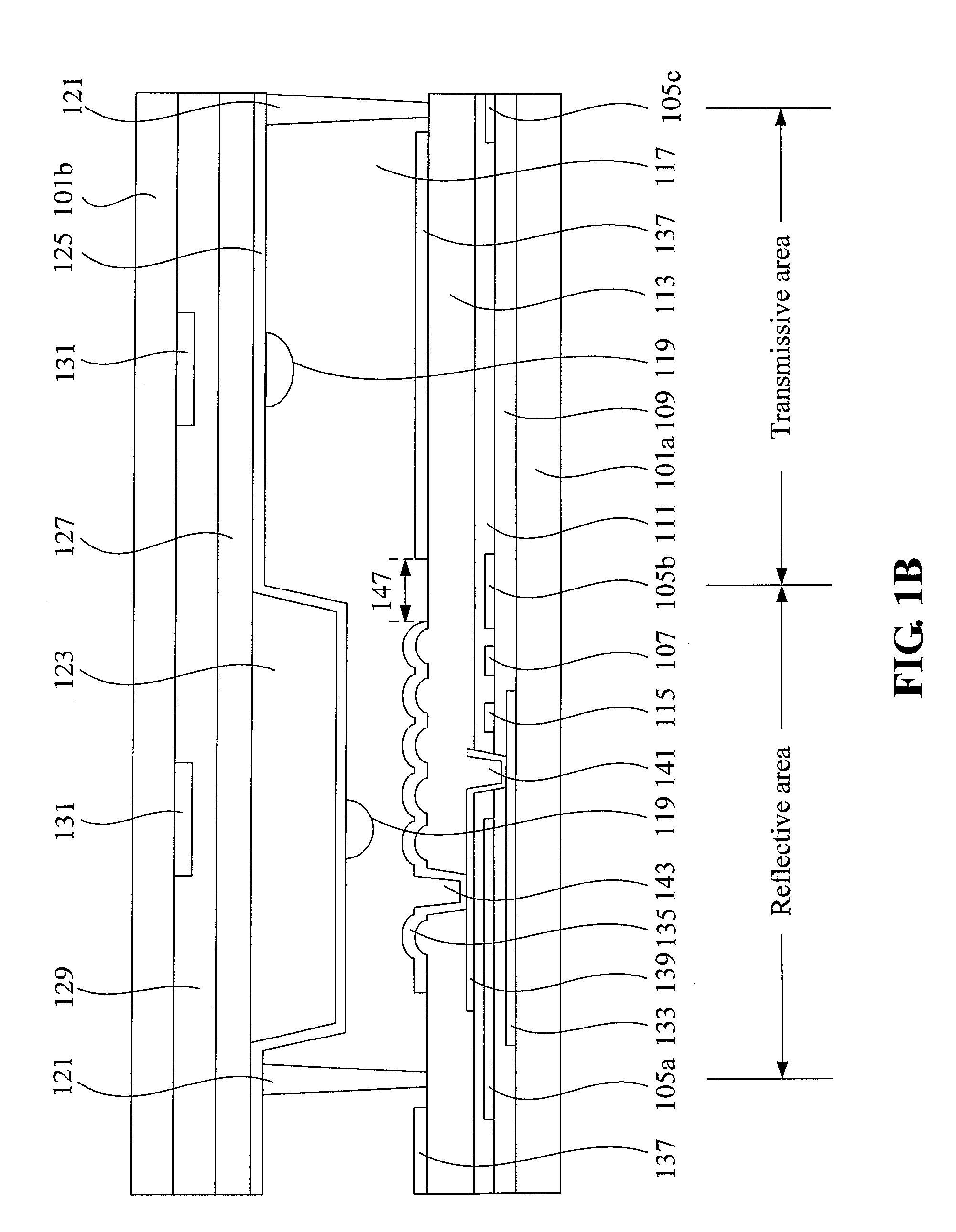
[0035]A display panel 15 disclosed in this invention comprises a pair of substrates 101a, 101b, a plurality of data lines 103, a plurality of common lines 105, a plurality of scan lines 107, a first dielectric layer 109, a second dielectric layer 111, a third dielectric layer 113, a switch element 115, a display media layer 117, an alignment element 119, a spacer 121, an organic dielectric layer 123, a common electrode 125, an overcoat 127, a color resist layer 129, and a black matrix (BM) 131. The corresponding relationships of which are depicted in FIGS. 1A and 1B.

[0036]As shown in FIG. 1B, the pair of substrates comprises a first substrate 101a and a second substrate 101b. The plurality of data lines 103 (not shown in FIG. 1B) are formed on the first substrate 101a, as are also the plurality of common lines 105a, 105b, 105c. The common lines 105a, 105b, 105c are substantially parallel to the scan lines 107, and interlaced with the data lines 103 to form a plurality of areas.

[0037...

second embodiment

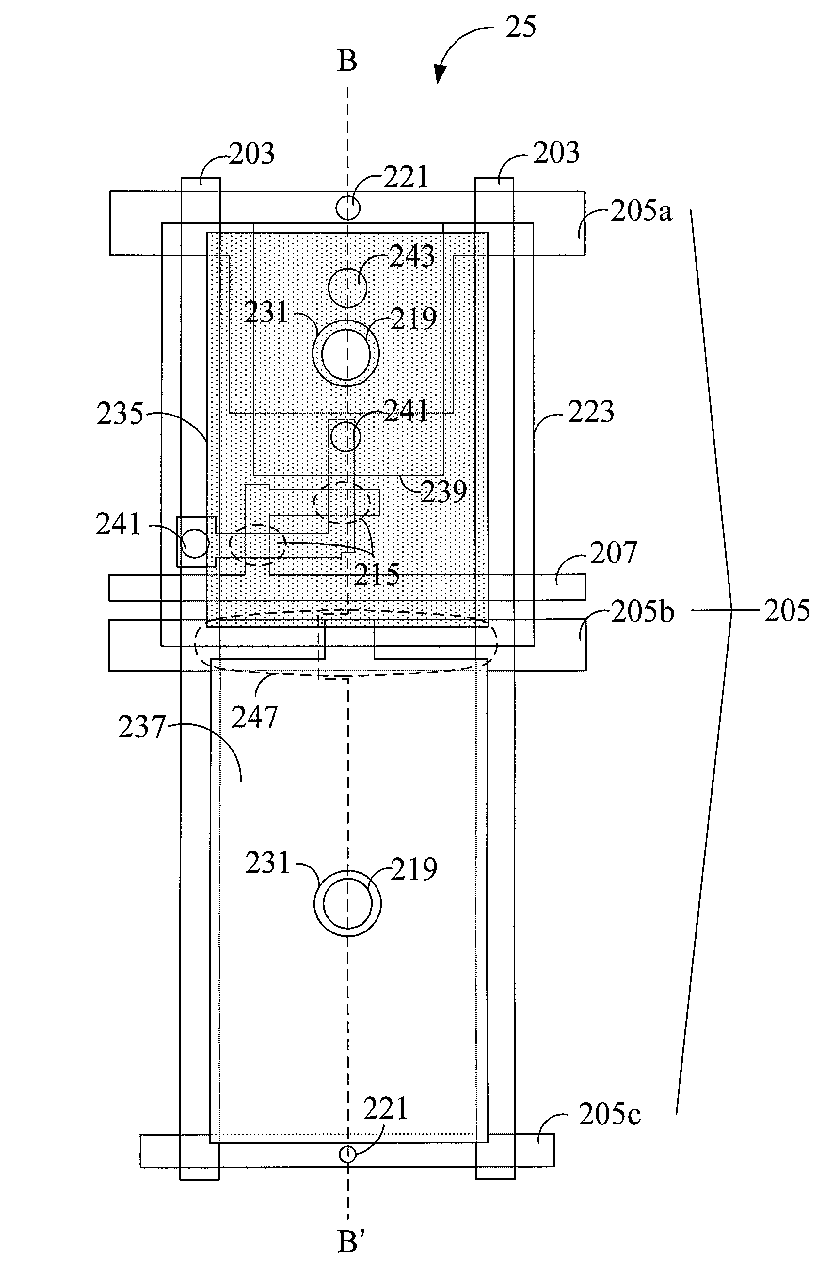
[0052]A display panel 25 disclosed in this invention comprises a pair of substrates 201a, 201b, a plurality of data lines 203, a plurality of common lines 205a, 205b, 205c, a plurality of scan lines 207, a first dielectric layer 209, a second dielectric layer 211, a third dielectric layer 213, a fourth dielectric layer 245, a switch element 215, a display media layer 217, an alignment element 219, a spacer 221, a common electrode 225, an overcoat 227, a color resist layer 229, and a black matrix (BM) 231. The corresponding relationships of which are depicted in FIGS. 2A and 2B.

[0053]In reference to FIG. 2B, the pair of substrates comprises a first substrate 201a and a second substrate 201b. The plurality of data lines 203 (not shown) are formed on the first substrate 201a, as are also the plurality of common lines 205a, 205b, 205c. The common lines 205a, 205b, 205c are substantially parallel to the scan lines 207, and interlaced with the data lines 203 to form a plurality of areas.

[...

third embodiment

[0068]A display panel 35 disclosed in this invention comprises a pair of substrates 301a, 301b, a plurality of data lines 303, a plurality of common lines 305, a plurality of scan lines 307, a first dielectric layer 309, a second dielectric layer 311, a third dielectric layer 313, a switch element 315, a display media layer 317, an alignment element 319, a spacer 321, an organic dielectric layer 323, a common electrode 325, an overcoat 327, a color resist layer 329, and a black matrix (BM) 331. The corresponding relationships of which are depicted in FIGS. 3A and 3B.

[0069]In reference to FIG. 3B, the pair of substrates comprises a first substrate 301a and a second substrate 301b. The plurality of data lines 303 (not shown in FIG. 3B) are formed on the first substrate 301a, as are also the plurality of common lines 305a, 305b, 305c. The common lines 305a, 305b, 305c are substantially parallel to the scan lines 307, and interlaced with the data lines 303 to form a plurality of areas.

[...


PUM

PropertyMeasurementUnit
electric potentialaaaaaaaaaa
voltageaaaaaaaaaa

Abstract

A display panel and an electro-optical device thereof are provided. The display panel comprises a pair of substrates, at least one data line, at least three common lines, at least one scan line, at least one switch element, a common electrode, and a display media layer. The pair of substrates comprises a first substrate and a second substrate. The data line and the three common lines are formed on the first substrate. The data line and the common lines interlace to form a plurality of areas. Each of the areas comprises an electrode. The electrodes are connected to each other to form a pixel electrode. The scan line is formed on the first substrate and under an electrode of one of the areas. The switch element is formed under an electrode of one of the areas, and comprises a source connected to the pixel electrode, a drain connected to the data line, and a gate \ connected to the scan line. The common electrode is formed on the second substrate, with a display media layer disposed between the two substrates.

Description

[0001]This application claims the benefits of Taiwan Application No. 096122036 filed on Jun. 20, 2007, the contents of which are herein incorporated by reference in their entirety.BACKGROUND OF THE INVENTION[0002]1. Field of the Invention[0003]The present invention relates to a display panel, an electro-optical device, and a method for fabricating the same and, more particularly, to improve the tilt conditions of the liquid crystal molecules in a display panel which eliminates the dark-state light leakage.[0004]2. Descriptions of the Related Art[0005]With the continuous advancement of technologies, a wide variety of electronic products have become indispensable. Particularly, the display devices play an important role in multimedia electronic products. Among various displays, the thin film transistor liquid crystal displays (TFT-LCDs) have some advantages, such as low power consumption, no radiation, small size, a flat panel profile, high resolution, and stable display quality. As a...

Claims


Application Information

Patent Timeline
Patent Type & Authority Applications(United States)
IPC IPC(8): G02F1/1343G02F1/1335G02F1/133
CPCG02F1/133555G02F1/133707G02F1/136286
Inventor FAN JIANG, SHIH-CHYUANLIN, CHING-HUANCHANG, CHIH-MING
Owner AU OPTRONICS CORP
Why Eureka
Try Eureka