Visual inspection apparatus for a wafer

Inactive Publication Date: 2008-12-25
ABLIC INC
View PDF1 Cites 3 Cited by
  • Summary
  • Abstract
  • Description
  • Claims
  • Application Information

AI Technical Summary

Benefits of technology

[0010]In such a manner, the visual inspection can be performed while considering the variation in gradation values for sampling areas, which is derived from the film thickness variation of the thin films between lots, in a lot, and in a wafer surface, thereby reducing d

Problems solved by technology

However a semiconductor device is, in general, manufactured by forming various thin films such as a silicon oxide film, a silicon nitride film, and polysilicon film on a semiconductor wafer, thickness variation in each of the various thin films occurs between lots, in a lot, and even in a wafer depending on the capacity of production equip

Method used


Image

  • Visual inspection apparatus for a wafer
  • Visual inspection apparatus for a wafer
  • Visual inspection apparatus for a wafer

Examples


Embodiment Construction

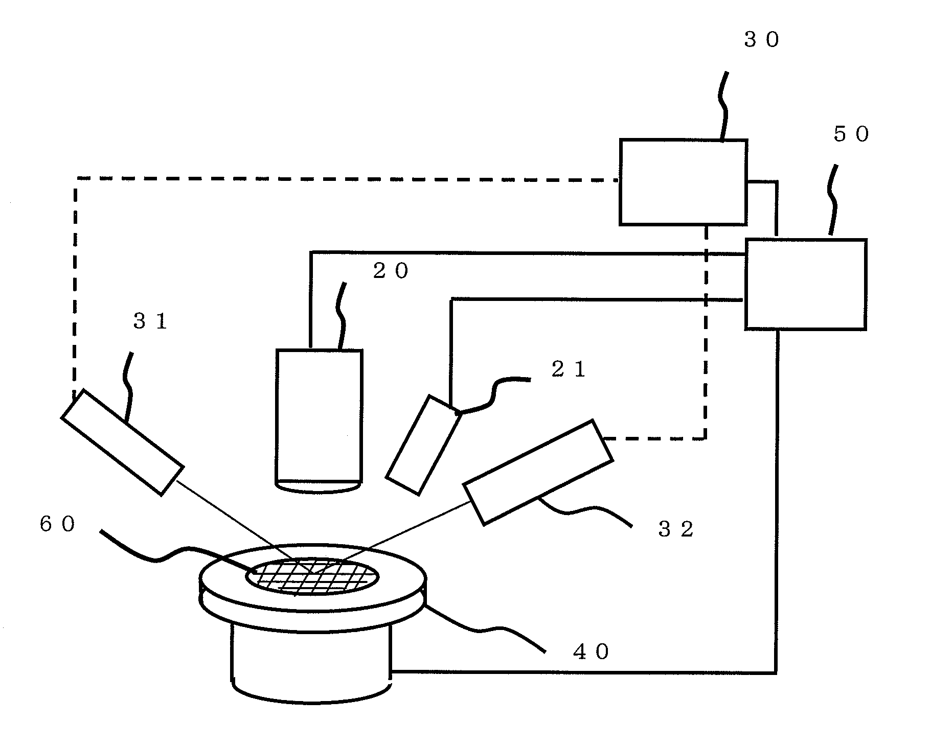
[0019]Hereinafter, an embodiment of the present invention will be described with reference to FIGS. 1A, 1B, 1C, 1D, and 2.

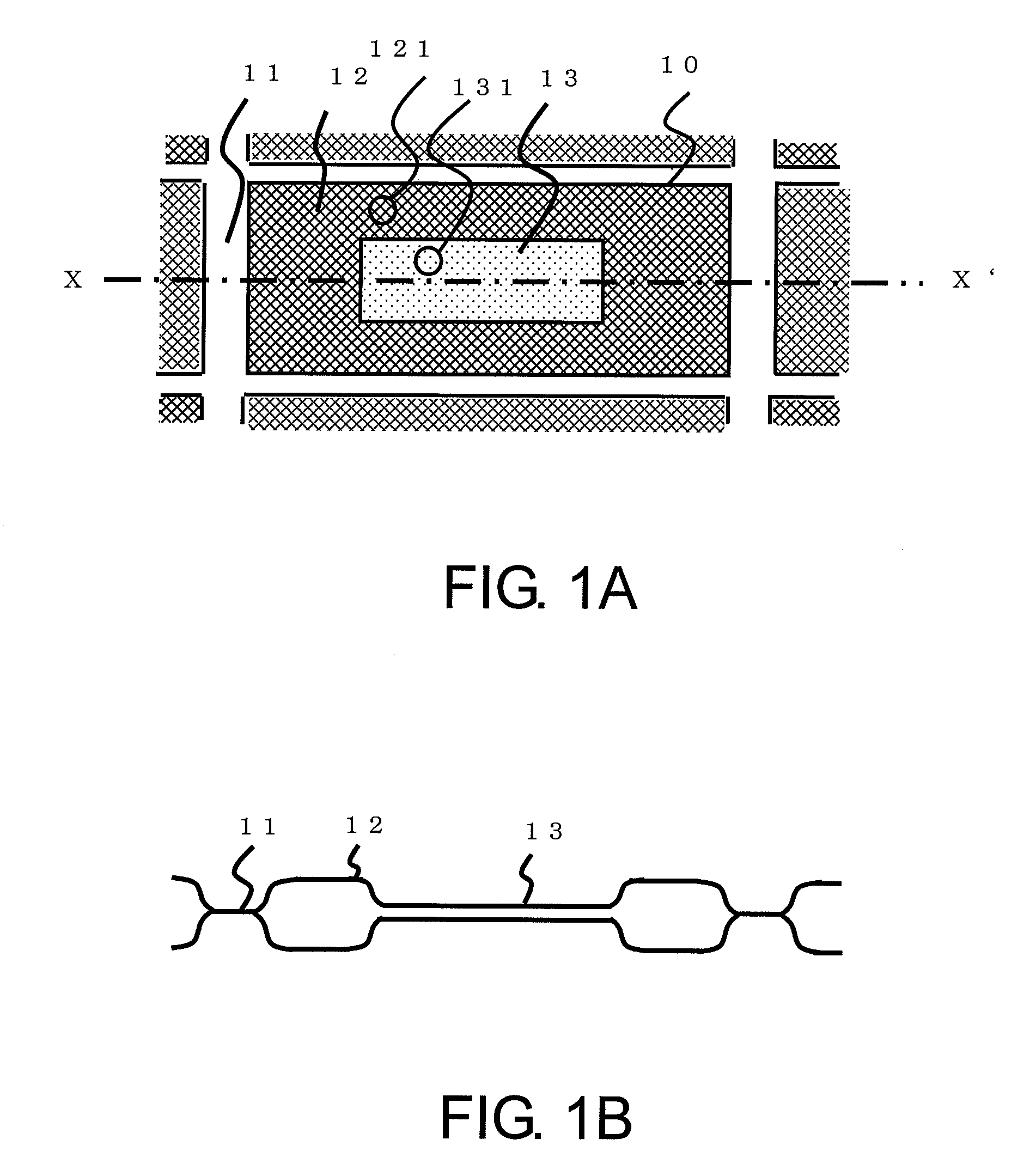
[0020]In an area of a chip 10 surrounded by a scribe line 11, a film thickness measurement point 121 of a first oxide film area 12 and a film thickness measurement point 131 of a second oxide film area 13 constituting the chip 10 with the first oxide film area 12 are set. Note that FIG. 1B illustrates a schematic sectional view taken along the line X-X′ of the chip of FIG. 1A.

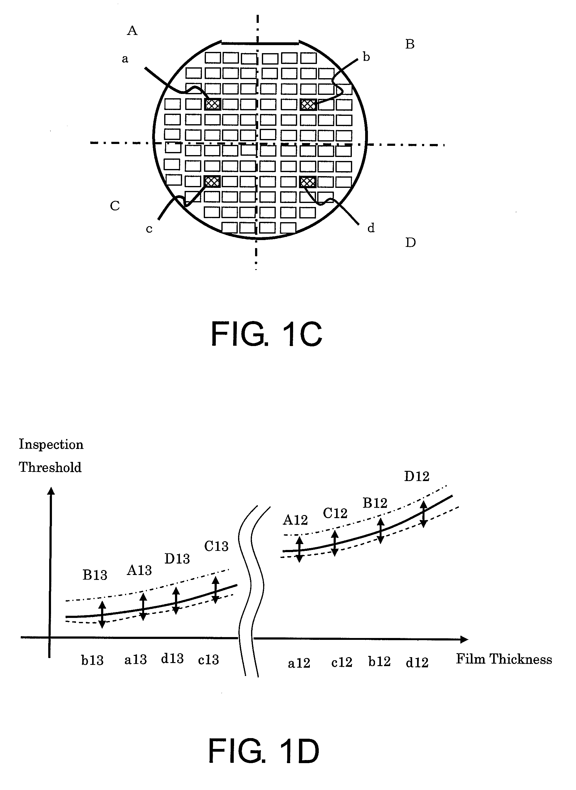
[0021]A wafer is divided into arbitrary areas each including chips. For example, in FIG. 1C, a wafer is divided into areas “A”, “B”, “C”, and “D”.

[0022]Subsequently, for each of the areas, at least one chip is selected to measure film thickness thereof. For example, in FIG. 1C, a chip “a” is selected for the area “A”, a chip “b” for the area “B”, a chip “c” for the area “C”, and a chip “d” for the area “D”.

[0023]In order to define a reference sample for comparing patterns of chips, a sensiti...


PUM


Abstract

Provided is a visual inspection apparatus for a semiconductor wafer, by which a threshold value optimal for inspection can be determined and visual inspection of each chip can be performed based on the threshold value, by obtaining in advance a table indicating a relation between a film thickness of a thin film in specific positions in the wafer and a gradation value for each sample area in the chip, measuring the film thickness of the thin film in the specific positions of the wafer to be inspected before inspecting the chip, and comparing the measured film thickness with the gradation value in the table.

Description

[0001]This application claims priority under 35 U.S.C. §119 to Japanese Patent Application No. JP2007-017602 filed Jan. 29, 2007, the entire content of which is hereby incorporated by reference.BACKGROUND OF THE INVENTION[0002]1. Field of the Invention[0003]The present invention relates to a visual inspection apparatus for performing visual inspection of a wafer and a semiconductor substrate, and more particularly, to a visual inspection apparatus for detecting defects on a wafer, which are generated in the manufacturing process of semiconductor integrated circuits.[0004]2. Description of the Related Art[0005]A method of comparing an inspection target image data with a reference image data to check the integrity of an inspection target based on any accidental difference between them is conventionally known as a visual inspection method for detecting conformity of pattern formed on an inspection target (a semiconductor wafer) and defects such as foreign substances and scratches on th...

Claims


Application Information

Patent Timeline
IPC IPC(8): G01B11/06
CPCG01B11/0641G01N21/211G01N21/8422G01N21/95607
Inventor TSURU, KIYOHIRO
Owner ABLIC INC
Why Eureka
Try Eureka