Multi-Level Controller with Smart Storage Transfer Manager for Interleaving Multiple Single-Chip Flash Memory Devices

a storage transfer manager and multi-level controller technology, applied in the direction of memory address/allocation/relocation, digital storage, instruments, etc., can solve the problems of mlc flash performance, reliability and durability may decrease, and the performance of nand flash is limited

Inactive Publication Date: 2008-12-25
SUPER TALENT TECH CORP
View PDF28 Cites 362 Cited by
  • Summary
  • Abstract
  • Description
  • Claims
  • Application Information

AI Technical Summary

Problems solved by technology

However, NAND flash has limitations.
One limitation of NAND flash is that when storing data (writing to flash), the flash can only write from ones (1) to zeros (0).
Another limitation is that NAND flash memory has a finite number of erase cycles between 10,000 to 1,000,000, after which the flash wear out and becomes unreliable.
But the performance, reliability and durability may decrease for MLC flash.
A similar problem could occur with other bus protocols, such as Serial AT-Attachment (SATA), integrated device electronics (IDE), and Peripheral Components Interconnect Express (PCIe).

Method used


Image

  • Multi-Level Controller with Smart Storage Transfer Manager for Interleaving Multiple Single-Chip Flash Memory Devices
  • Multi-Level Controller with Smart Storage Transfer Manager for Interleaving Multiple Single-Chip Flash Memory Devices
  • Multi-Level Controller with Smart Storage Transfer Manager for Interleaving Multiple Single-Chip Flash Memory Devices

Examples


Embodiment Construction

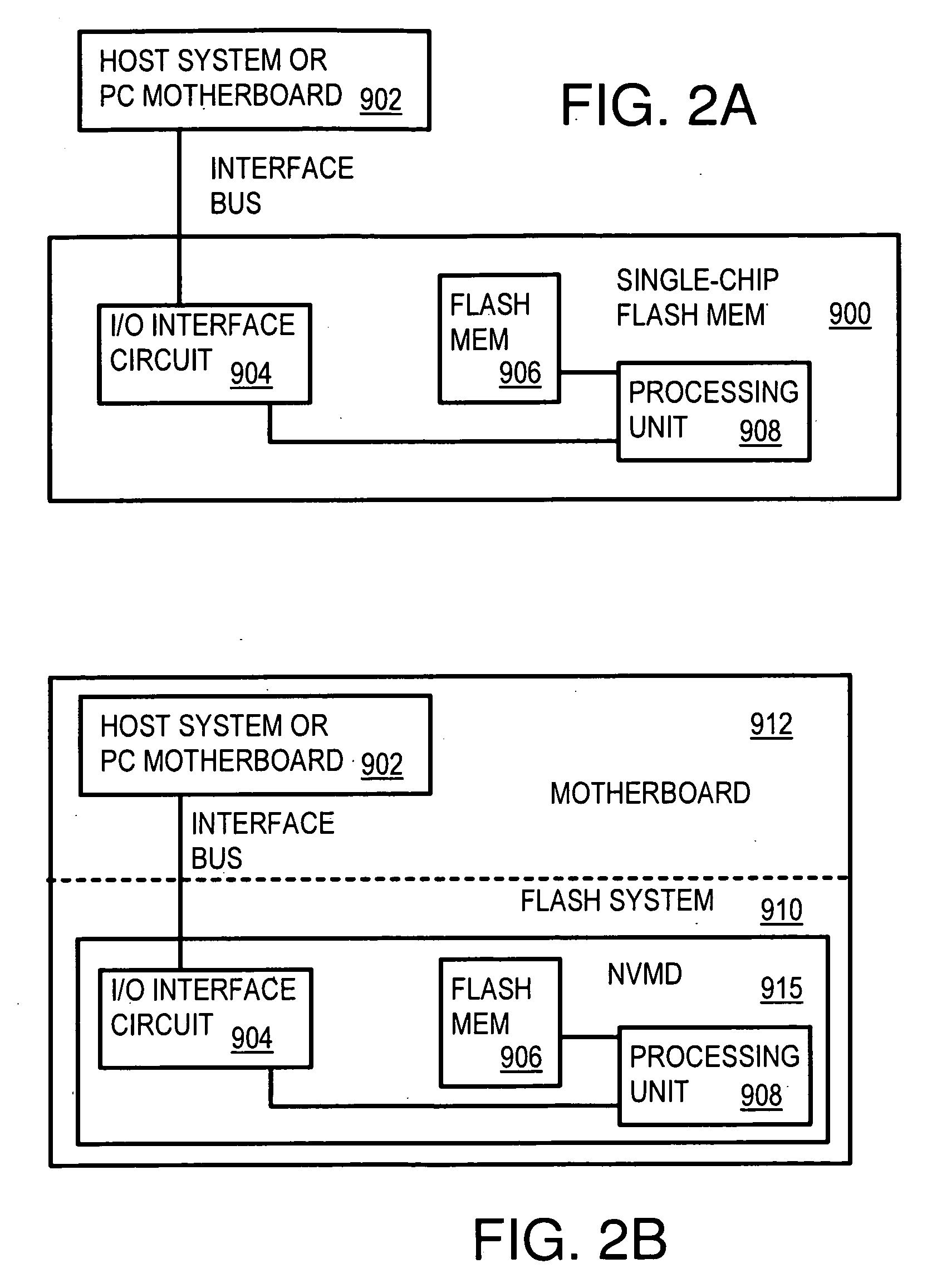
[0041]The present invention relates to an improvement in solid-state flash drives. The following description is presented to enable one of ordinary skill in the art to make and use the invention as provided in the context of a particular application and its requirements. Various modifications to the preferred embodiment will be apparent to those with skill in the art, and the general principles defined herein may be applied to other embodiments. Therefore, the present invention is not intended to be limited to the particular embodiments shown and described, but is to be accorded the widest scope consistent with the principles and novel features herein disclosed.

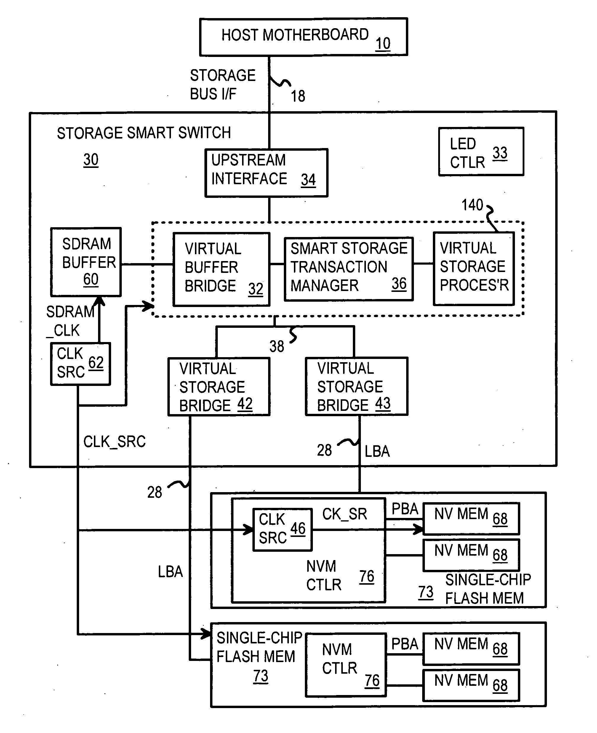
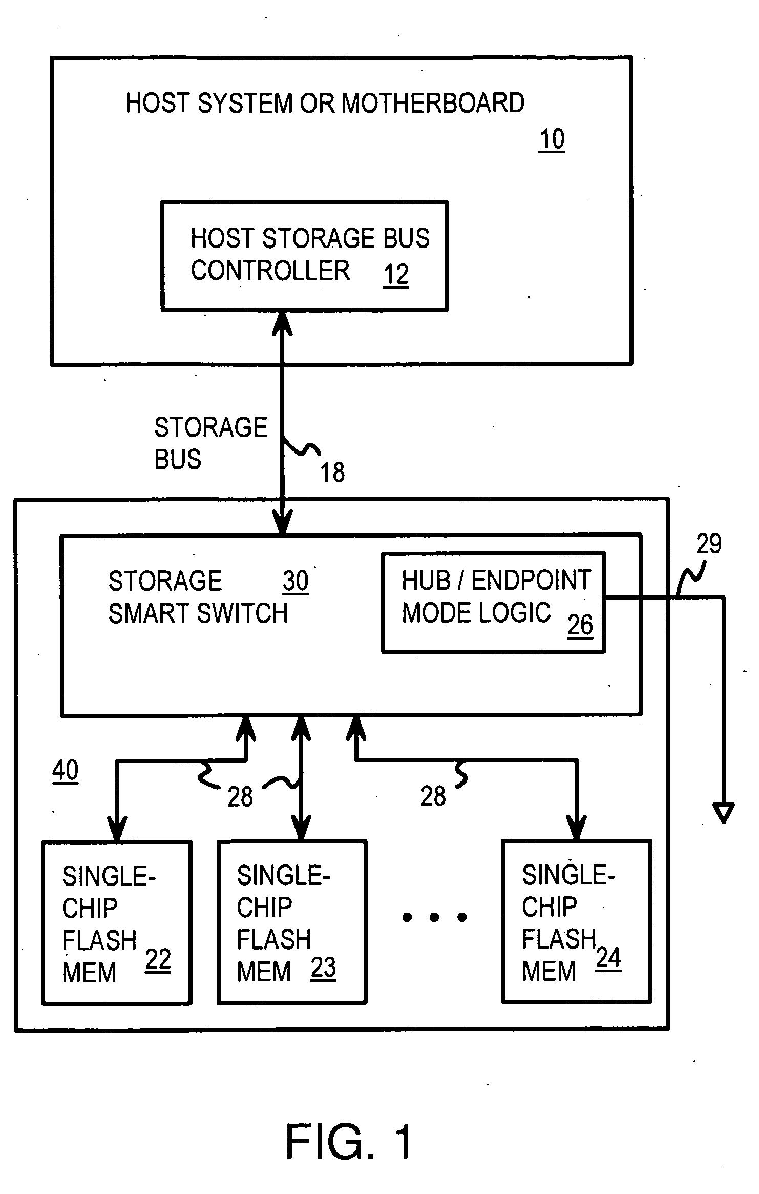
[0042]FIG. 1 is a block diagram of a switch that aggregates and virtualizes multiple flash-memory endpoints. Host controller 12 for host 10 sends transactions over storage bus 18 to multi-flash device 40. Smart storage switch 30 on multi-flash device 40 receives and responds to transaction from host 10 over storage bus 18.

[00...


PUM


Abstract

A solid-state disk (SSD) has a smart storage switch with a smart storage transaction manager that re-orders host commands for accessing downstream single-chip flash-memory devices. Each single-chip flash-memory device has a lower-level controller that converts logical block addresses (LBA) to physical block addresses (PBA) that access flash memory blocks in the single-chip flash-memory device. Wear-leveling and bad block remapping are preformed by each single-chip flash-memory device, and at a higher level by a virtual storage processor in the smart storage switch. Virtual storage bridges between the smart storage transaction manager and the single-chip flash-memory devices bridge LBA transactions over LBA buses to the single-chip flash-memory devices. Data striping and interleaving among multiple channels of the single-chip flash-memory device is controlled at a high level by the smart storage transaction manager, while further interleaving and remapping may be performed within each single-chip flash-memory device.

Description

RELATED APPLICATIONS[0001]This application is a continuation-in-part (CIP) of “High Integration of Intelligent Non-Volatile Memory Devices”, Ser. No. 12 / 054,310, filed Mar. 24, 2008, which is a CIP of “High Endurance Non-Volatile Memory Devices”, Ser. No. 12 / 035,398, filed Feb. 21, 2008, which is a CIP of “High Speed Controller for Phase Change Memory Peripheral Devices”, U.S. application Ser. No. 11 / 770,642, filed on Jun. 28, 2007, which is a CIP of “Local Bank Write Buffers for Acceleration a Phase Change Memory”, U.S. application Ser. No. 11 / 748,595, filed May 15, 2007, which is CIP of “Flash Memory System with a High Speed Flash Controller”, application Ser. No. 10 / 818,653, filed Apr. 5, 2004, now U.S. Pat. No. 7,243,185.[0002]This application is also a CIP of co-pending U.S. Patent Application for “Multi-Channel Flash Module with Plane-Interleaved Sequential ECC Writes and Background Recycling to Restricted-write Flash Chips”, Ser. No. 11 / 871,627, filed Oct. 12, 2007, and is al...

Claims


Application Information

Patent Timeline
Patent Type & Authority Applications(United States)
IPC IPC(8): G06F12/02
CPCG06F3/0613G06F3/0616G06F3/064G06F3/0658G06F3/0664G06F3/0688G06F12/0246G06F2212/7201G06F2212/7208G06F2212/7211G11C13/0004
Inventor MA, ABRAHAM C.CHOW, DAVID Q.LEE, CHARLES C.YU, FRANK
Owner SUPER TALENT TECH CORP
Why Eureka
Try Eureka