Liquid crystal display panel manufacturing method and device

a technology of liquid crystal display panel and manufacturing method, which is applied in the manufacture of electrode systems, electric discharge tubes/lamps, instruments, etc., can solve the problems of more serious problems, glass substrate damage, and uniform gaps in display cells

Inactive Publication Date: 2009-01-08
FUJITSU LTD
View PDF6 Cites 10 Cited by
  • Summary
  • Abstract
  • Description
  • Claims
  • Application Information

AI Technical Summary

Problems solved by technology

The method of physically pressing the pair of glass substrates on both sides cannot avoid disuniform pressure in the glass substrates and has a problem that this causes disuniform gaps of the display cells.
It is also a problem that when foreign objects, such as particles, etc., are present on the glass substrates, the glass substrates are damaged by the press.
As the liquid crystal display device is thinned, the above-described problems are more serious.
When ...

Method used


Image

  • Liquid crystal display panel manufacturing method and device
  • Liquid crystal display panel manufacturing method and device
  • Liquid crystal display panel manufacturing method and device

Examples


first embodiment

A First Embodiment

[0018]The liquid crystal display panel manufacturing method according to a first embodiment will be explained with reference to FIGS. 1 to 3.

[0019]FIGS. 1A and 1B are views of the steps of the liquid crystal display panel manufacturing method according to the present embodiment, FIGS. 2A and 2B are views of the steps of the liquid crystal display panel manufacturing method according to the present embodiment, and FIGS. 3A to 3C are views of the steps of the liquid crystal display panel manufacturing method according to the present embodiment.

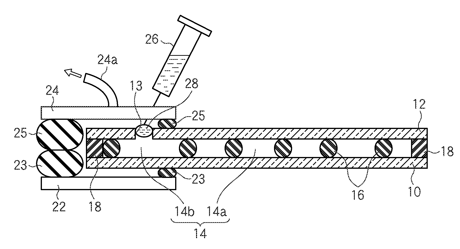
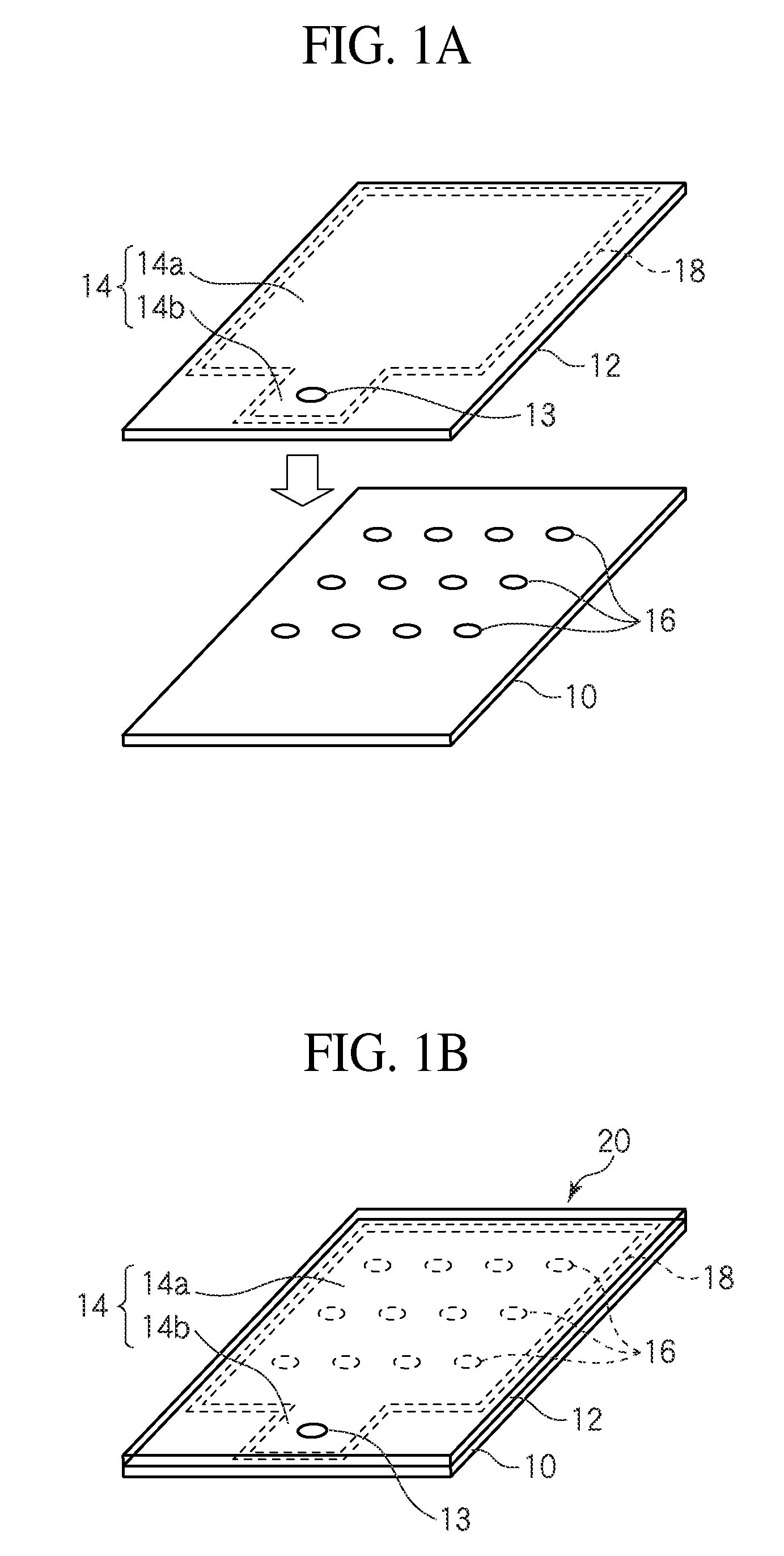
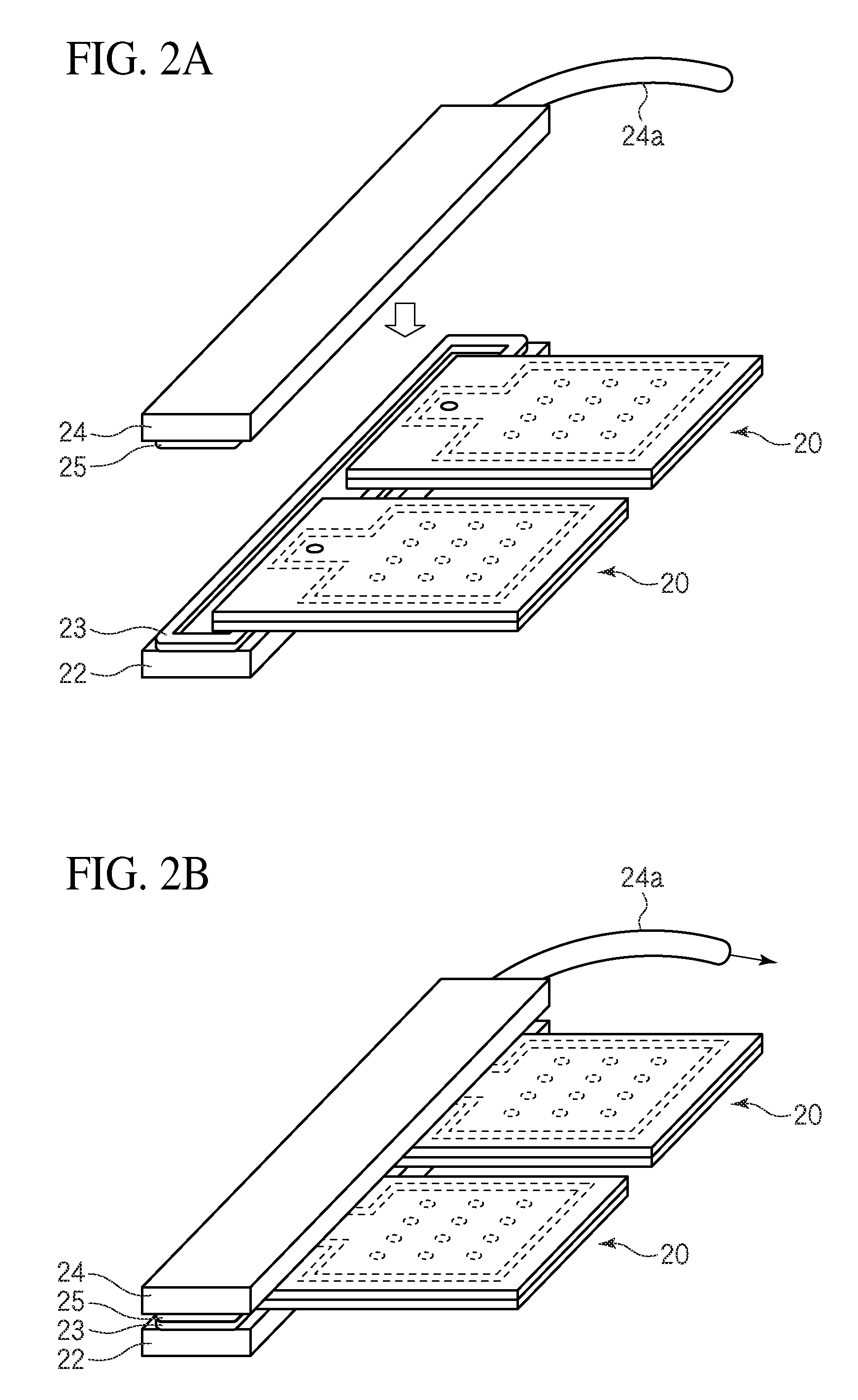
[0020]First, as illustrated in FIG. 1A, a pair of glass substrate 10, 12 are prepared. The glass substrates 10, 12 have the size of, e.g., a 0.2 mm thickness, a 80 mm longitudinal length and a 100 mm lateral length.

[0021]Spacers 16 are distributed on one glass substrate 10 in the cell region 14 where cells are to be formed. The spacers 16 are distributed for uniformly retaining a prescribed distance in the cell region 14 when t...

second embodiment

A Second Embodiment

[0038]The liquid crystal display panel manufacturing method according to a second embodiment will be explained with reference to FIGS. 4 to 8.

[0039]FIGS. 4A to 4C are views of the steps of the liquid crystal display panel manufacturing method according to the present embodiment, FIGS. 5A and 5B are views of the steps of the liquid crystal display panel manufacturing method according to the present embodiment, FIG. 6 is a view of the step of the liquid crystal display panel manufacturing method according to the present embodiment, FIGS. 7A and 7B are views of the steps of the liquid crystal display panel manufacturing method according to the present embodiment, and FIGS. 8A and 8B are views of the steps of the liquid crystal display panel manufacturing method according to the present embodiment.

[0040]The liquid crystal display panel according to the present embodiment is basically the same as the liquid crystal display panel according to the first embodiment but is...


PUM


Abstract

A liquid crystal display panel 20 is manufactured by applying a seal agent 19 to at least of a pair of substrates 10, 12, enclosing the cell region 14; opposing the pair of substrates 10, 12 at a prescribed gap to define a cell space 14; depressurizing the interior of the cell space 14 through an opening 13 formed in at least one of the pair of substrates 10, 12 to thereby securely bond the pair of substrate 10, 12 to each other; and injecting a liquid crystal into the cell space 14. The atmospheric pressure is applied to the pair of substrates 10, 12, whereby a uniform external pressure is applied, and the glass substrates can be securely bonded to each other in good condition.

Description

CROSS REFERENCE TO RELATED APPLICATIONS[0001]This application is a Continuation of International Application No. PCT / JP2006 / 304343, with an international filing date of Mar. 7, 2006, which designating the United States of America, the entire contents of which are incorporated herein by reference.TECHNICAL FIELD[0002]The present invention relates to a liquid crystal display panel manufacturing method and device for manufacturing a liquid crystal display panel.BACKGROUND[0003]Recently, liquid crystal display devices using liquid crystal materials are popular in the daily life.[0004]As methods of forming liquid crystal display devices, various modes such as TN (Twisted Nematic) mode liquid crystal, STN (Super Twisted Nematic) mode liquid crystal, TSTN (Triple Super Twisted Nematic) mode liquid crystal, etc., are used. In any one of such different modes, to manufacture the liquid crystal display device, a pair of glass substrates with transparent electrodes formed on are bonded, a liqui...

Claims


Application Information

Patent Timeline
IPC IPC(8): G02F1/1339H01J9/26H01L21/02
CPCG02F1/1341G02F1/1303
Inventor KUROSAKI, YOSHIHISATOMITA, JUNJI
Owner FUJITSU LTD
Why Eureka
Try Eureka