Reconfigurable semiconductor structure processing using multiple laser beam spots

a semiconductor structure and laser beam technology, applied in the direction of semiconductor/solid-state device details, manufacturing tools, welding/soldering/cutting articles, etc., can solve the problems of difficult to achieve large throughput gains, link banks may not be straight rows, link runs may not be processed with continuous motion,

Inactive Publication Date: 2009-01-08
ELECTRO SCI IND INC
View PDF6 Cites 33 Cited by
  • Summary
  • Abstract
  • Description
  • Claims
  • Application Information

AI Technical Summary

Problems solved by technology

During their fabrication process, ICs (integrated circuits) often incur defects for various reasons.
In addition, link banks, and link runs may not be straight rows and may not be processed with continuous motion.
Improvements in these areas will continue; however, practical limitations associated with these parameters make this a difficult way to achieve large throughput gains.
Increasing stage acceleration introduces additional vibrations and generates heat, both of which can decrease system accuracy.
Significantly increasing the stage acceleration and bandwidth, without diminishing the positional accuracy or increasing the system footprint, is a challenging and costly engineering endeavor, and

Method used


Image

  • Reconfigurable semiconductor structure processing using multiple laser beam spots
  • Reconfigurable semiconductor structure processing using multiple laser beam spots
  • Reconfigurable semiconductor structure processing using multiple laser beam spots

Examples


Embodiment Construction

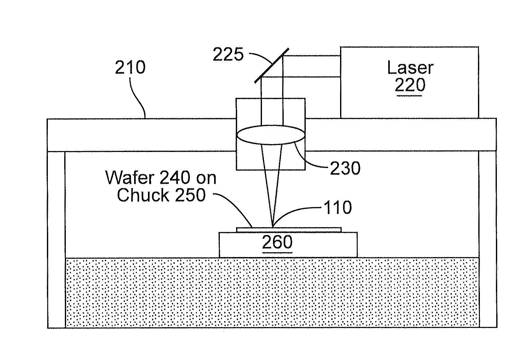
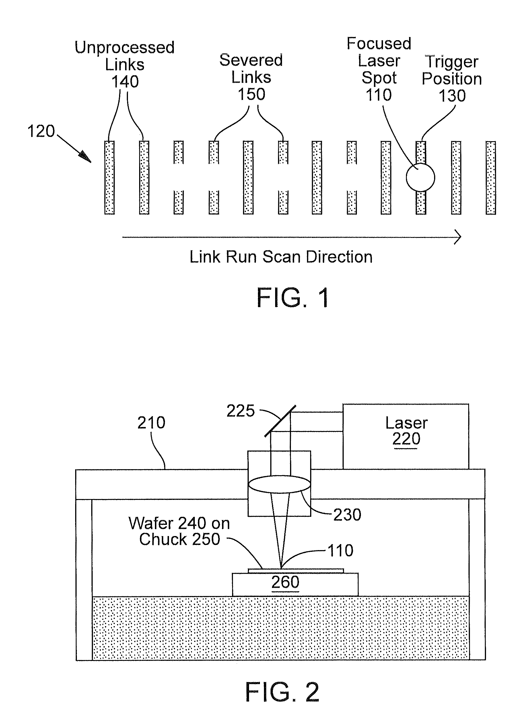
[0040]With reference to the above-listed drawings, this section describes particular embodiments and their detailed construction and operation. The principles, methods, and systems disclosed below have general applicability for processing any structure on or within a semiconductor substrate using laser radiation for any purpose. While the examples and embodiments that follow are described in the context in which those structures are laser-severable links on or within an IC (e.g., memory device, logic device, optical or optoelectronic device including LEDs, and microwave or RF devices), other structures besides laser-severable links can be processed in the same or similar manner, and the teachings set forth herein are equally applicable to the laser processing of other types of structures, such as electrical structures that become conductive as a result of laser radiation, other electrical structures, optical or electro-optical structures, and mechanical or electro-mechanical structu...


PUM

PropertyMeasurementUnit
Electrical conductivityaaaaaaaaaa
Concentrationaaaaaaaaaa
Electrical conductoraaaaaaaaaa

Abstract

Methods and systems selectively irradiate structures on or within a semiconductor wafer using multiple laser beams. The structures may be laser-severable conductive links, and the purpose of the irradiation may be to sever selected links. The structures are arranged in rows and may be processed in either an on-axis mode or a cross-axis mode. In the on-axis mode, the beam spots fall on structures in the same row as they move along the row. In the cross-axis mode, the beam spots fall on structures in different rows as they move along the rows.

Description

RELATED APPLICATIONS[0001]This application is a continuation-in-part of each of the following three U.S. Patent Applications: (1) No. 11 / 051,958, filed Feb. 4, 2005, entitled “Semiconductor Structure Processing Using Multiple Laser Beam Spots Spaced On-Axis with Cross-Axis Offset” issuing Sep. 16, 2008 as U.S. Pat. No. 7,425,471, which claims priority to U.S. Provisional Application No. 60 / 580,917, filed Jun. 18, 2004, entitled “Multiple-Beam Semiconductor Link Processing”; (2) No. 11 / 481,562, filed Jul. 5, 2006, entitled “Systems and Methods for Alignment of Laser Beam(s) for Semiconductor Link Processing,” which is a continuation-in-part of the above-referenced U.S. patent application Ser. No. 11 / 051,265; and (3) No. 11 / 499,394, filed Aug. 3, 2006, entitled “Systems and Methods for Distinguishing Reflections of Multiple Laser Beams for Calibration for Semiconductor Link Processing,” which is also a continuation-in-part of the above-referenced U.S. patent application Ser. No. 11 / 05...

Claims


Application Information

Patent Timeline
IPC IPC(8): H01L21/268B23K26/08
CPCB23K26/0635B23K26/0656B23K26/067B23K26/0676B23K26/0853H01L23/5258B23K2203/10B23K2203/12B23K2203/14H01L21/76894B23K2201/40B23K26/0624B23K26/066B23K2101/40B23K2103/10B23K2103/12B23K2103/14H01L2924/0002H01L2924/00
Inventor BRULAND, KELLY J.BAIRD, BRIAN W.LO, HO WAISWARINGEN, STEPHEN N.EVANS, FRANK G.
Owner ELECTRO SCI IND INC
Why Eureka
Try Eureka