Output buffer circuit
a buffer circuit and output circuit technology, applied in the direction of oscillator generators, pulse manipulation, pulse technique, etc., can solve the problems of the inability to adjust the rise and fall times of signals, and the loss of transmission lines to deteriorate the signal waveform
- Summary
- Abstract
- Description
- Claims
- Application Information
AI Technical Summary
Benefits of technology
Problems solved by technology
Method used
Image

Examples
embodiment 1
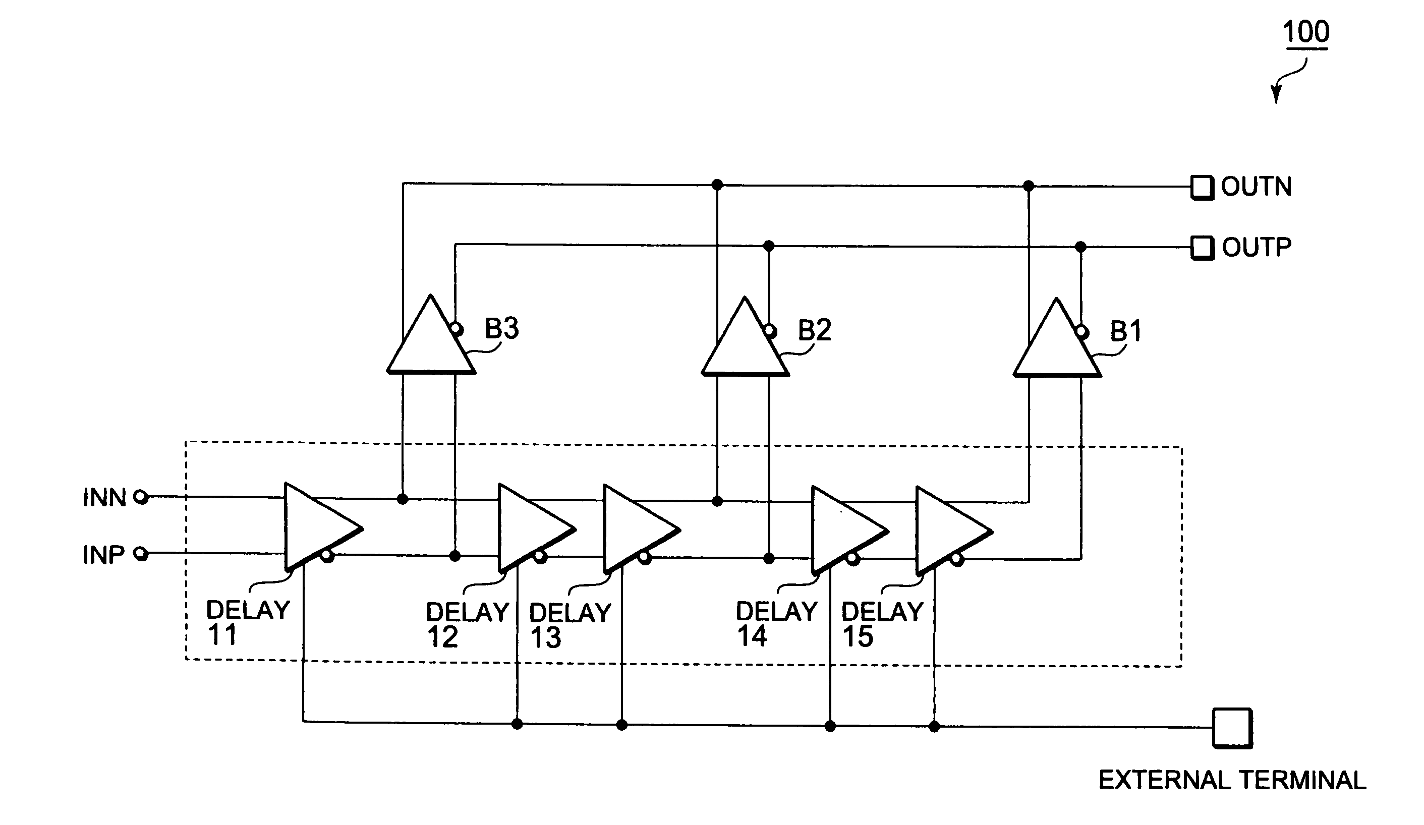
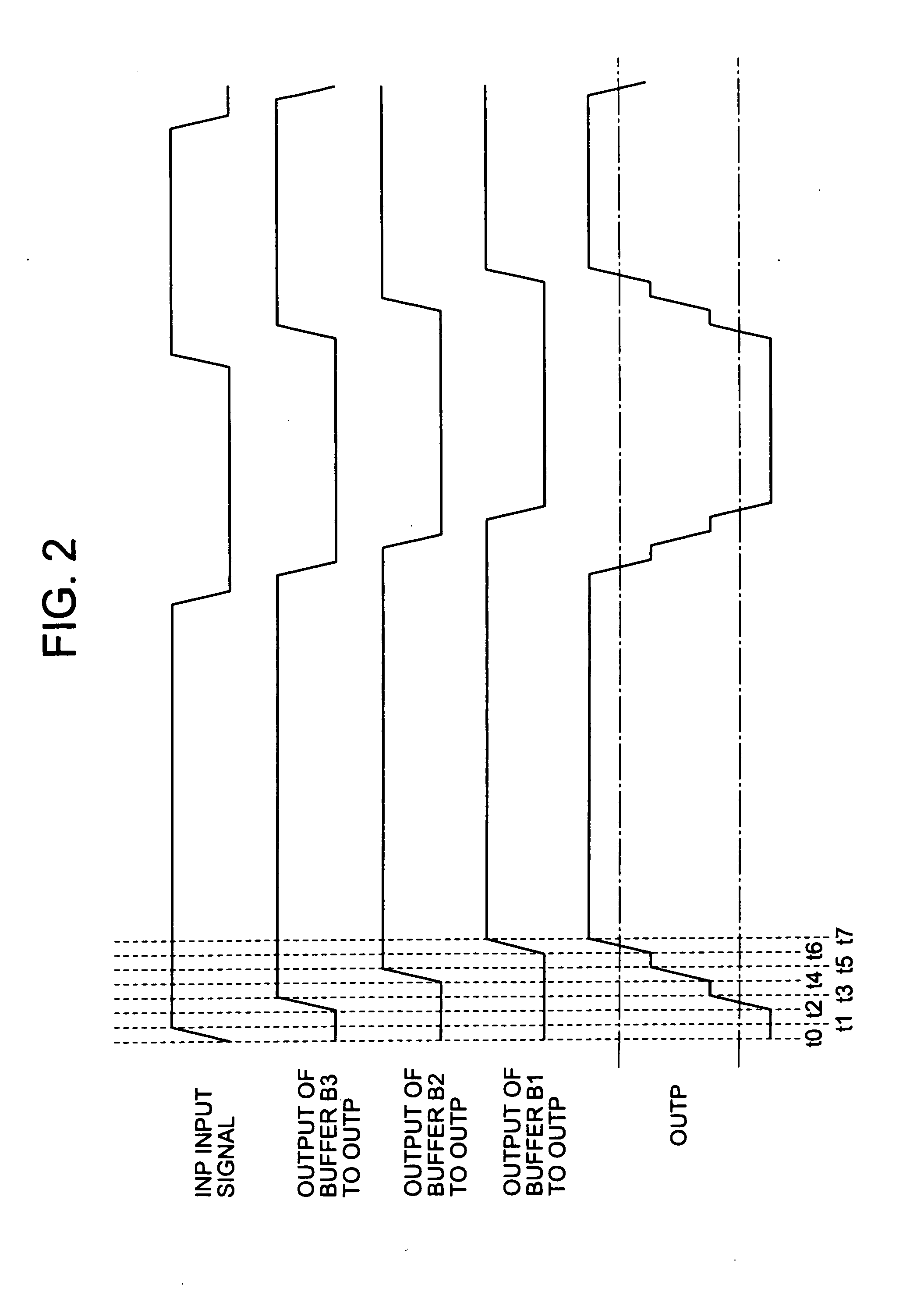
[0029]FIG. 1 is a block diagram showing an output buffer circuit 100 according to Embodiment 1 of the present invention. As shown in FIG. 1, the output buffer circuit 100 according to this embodiment includes a first output buffer (herein after referred to as output buffer B2), a second output buffer (herein after referred to as output buffer B1), and a third output buffer B3, a plurality of delay elements DELAY11, DELAY12, DELAY13, DELAY14, and DELAY15 corresponding to delay elements, differential input terminals (INP / INN), and differential output terminals (OUTP / OUTN). When a first delay path corresponds to the delay element DELAY11 in the plurality of delay elements DELAY11 to DELAY15, a second delay path corresponds to the delay elements DELAY12 and DELAY13. When the first delay path corresponds to the delay elements DELAY12 and DELAY13, the second delay path corresponds to the delay elements DELAY14 and DELAY15. Note that the differential input terminals (INP / INN) include the n...
embodiment 2
[0043]FIG. 4 shows an output buffer circuit 200 according to Embodiment 2 of the present invention. In FIG. 4, sections common to those of FIG. 1 are denoted by the same reference symbols and thus a detailed description thereof is omitted here. In the output buffer circuit 100 according to Embodiment 1, the signal for adjusting rising and falling times is outputted from each of the output buffers B1 to B3 provided between the delay elements coupled in series. The output buffer circuit 200 according to this embodiment has a structure in which multiplexing drivers MUX21, MUX22, and MUX23 are further provided to input in-phase data signals to the output buffers B1 to B3. Hereinafter, only the coupling relationship and operation of each of the multiplexing drivers MUX21, MUX22, and MUX23 are described.
[0044]Input terminals of the multiplexing driver MUX21 are coupled to the differential input terminals (INP / INN) and the output terminals of the delay element DELAY11. Output terminals of ...
embodiment 3
[0049]FIG. 5 shows an output buffer circuit 300 according to Embodiment 3 of the present invention. In FIG. 5, sections common to those of FIGS. 1 and 4 are denoted by the same reference symbols and thus a detailed description thereof is omitted here. In the output buffer circuit 300, a third output buffer (including, for example, output buffers B4 and B5), delay elements DELAY31, DELAY32, DELAY33, DELAY34, DELAY35, DELAY36, DELAY37, and DELAY38, and multiplexing drivers MUX31 and MUX32 are further provided at the subsequent stage of the output buffer circuit 200.
[0050]In the output buffer circuit 300, the delay elements DELAY31 to DELAY38 are coupled in series after the delay elements DELAY11 to DELAY15. Each of the delay elements DELAY11 to DELAY15 and each of the delay elements DELAY31 to DELAY38 have a non-inverted output terminal and an inverted output terminal, respectively. Each of the delay elements outputs a normal side signal of differential signals from the non-inverted o...
PUM
 Abstract
Description
Claims
Application Information
 - R&D
- Intellectual Property
- Life Sciences
- Materials
- Tech Scout
- Unparalleled Data Quality
- Higher Quality Content
- 60% Fewer Hallucinations
Browse by: Latest US Patents, China's latest patents, Technical Efficacy Thesaurus, Application Domain, Technology Topic, Popular Technical Reports.
© 2025 PatSnap. All rights reserved.Legal|Privacy policy|Modern Slavery Act Transparency Statement|Sitemap|About US| Contact US: help@patsnap.com